Product Table
| Property | Specification |
|---|---|
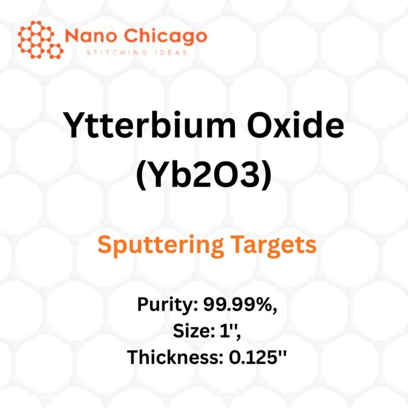
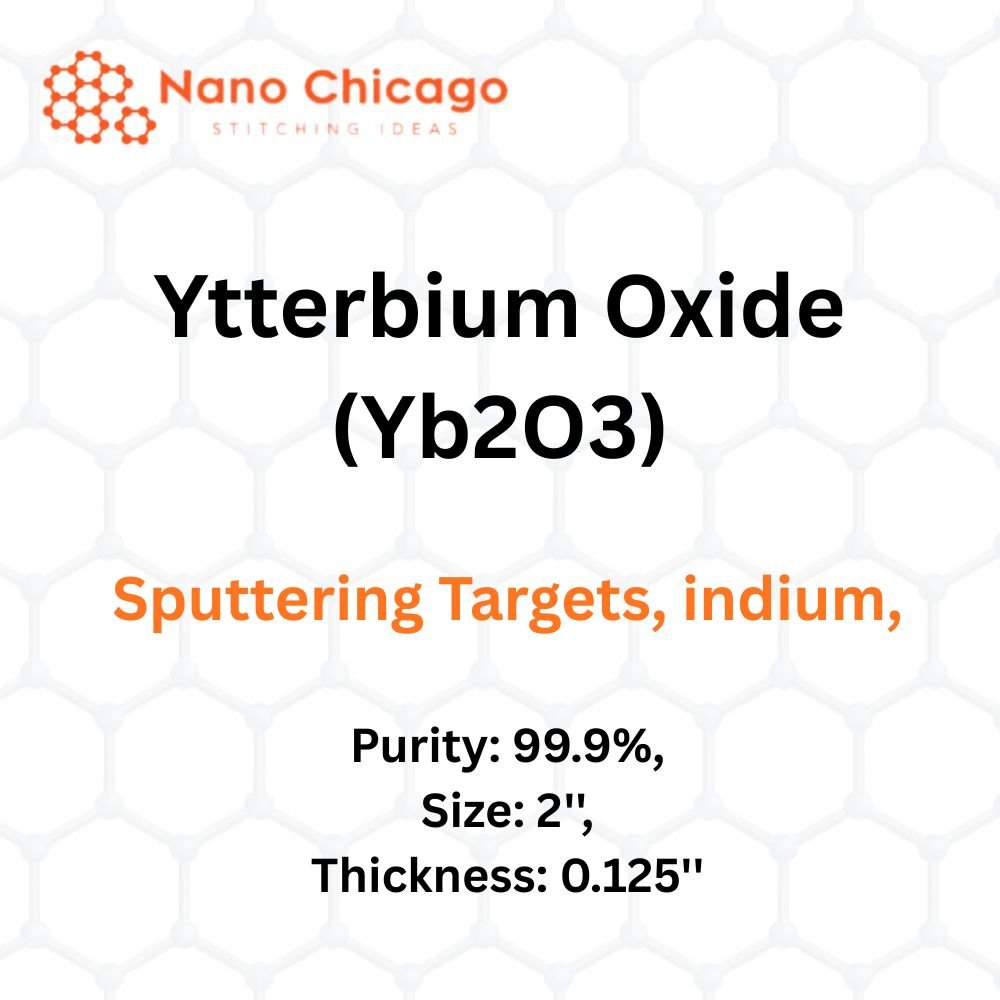
| Material | Ytterbium Oxide (Yb₂O₃), Indium Bonded |
| Purity | 99.9% |
| Size | 2” |
| Thickness | 0.125” |
| Form | Sputtering Target |
Description
Ytterbium Oxide (Yb₂O₃) sputtering targets—indium bonded—are used for high-quality thin-film deposition across a wide variety of substrate shapes and sizes. The sputtering process offers repeatability, scalability from R&D to high-volume production, and precise control over microstructure and film growth. Chemical reactions may occur on the target, during particle transport, or directly on the substrate depending on process parameters.
Applications
-
Thin Film Deposition: Transfers target material onto substrates such as silicon wafers through controlled sputtering.
-
Semiconductor Etching: Used in processes requiring high anisotropy where selectivity is less critical.
-
Material Analysis: Applied in SIMS and similar analytical techniques for composition profiling and impurity detection.
-
Space Research: Supports studies of space weathering affecting airless planetary bodies like the Moon and asteroids.