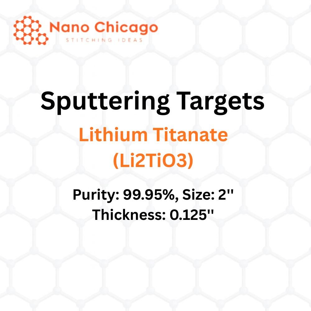
Lithium Titanate (Li₂TiO₃) Sputtering Targets
Purity: 99.95% Size: 4″ Thickness: 0.250″
Sputtering is a proven thin-film deposition technology capable of coating a wide range of materials onto diverse substrate shapes and sizes. Processes using sputter targets are highly repeatable and can be scaled from small R&D applications to medium- and large-area production batches. Depending on the process parameters, chemical reactions may occur on the target surface, during in-flight transport, or on the substrate itself. Although sputter deposition involves many variables, this complexity allows experts extensive control over film growth and microstructure.
Applications of Sputtering Targets
- Thin-film deposition:
Sputtering targets are used to erode material from a “target” and deposit it onto a “substrate,” such as a silicon wafer. - Semiconductor etching:
Semiconductor sputtering targets are used for sputter etching, preferred when a high degree of anisotropy is required and selectivity is not a primary concern. - Analytical applications:
Sputtering is used to gradually remove material for analysis.
A key example is Secondary Ion Mass Spectroscopy (SIMS), where the target is sputtered at a constant rate and the sputtered atoms are analyzed via mass spectrometry. This allows determination of material composition and detection of extremely low-level impurities. - Space science:
Sputtering also occurs naturally as a form of space weathering, altering the physical and chemical properties of airless bodies such as the Moon and asteroids.

