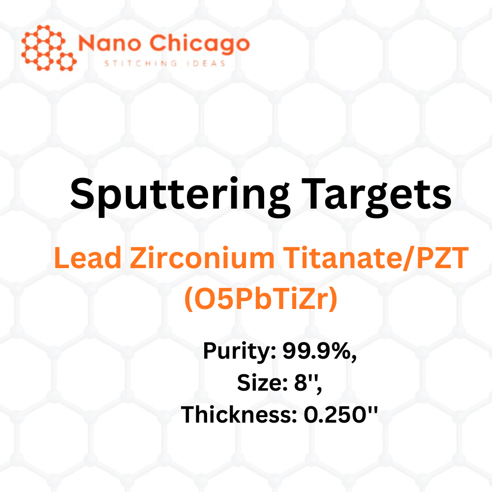
Lead Zirconium Titanate/PZT (O5PbTiZr) Sputtering Targets
| Property | Specification |
|---|---|
| Purity | 99.9% |
| Size | 8” |
| Thickness | 0.250” |
Sputtering is a proven technology capable of depositing thin films from a wide variety of materials onto diverse substrate shapes and sizes. The process using sputter targets is repeatable and can be scaled from small research and development projects to production batches involving medium to large substrate areas. Depending on the process parameters, the chemical reaction can occur on the target surface, in-flight, or on the substrate. Although sputter deposition involves many parameters and is complex, it gives experts a high degree of control over the growth and microstructure of the film.
Applications of Sputtering Targets
Sputtering targets are used for film deposition. The deposition created by sputter targets is a method of forming thin films by sputtering, which involves eroding material from a “target” onto a “substrate,” such as a silicon wafer.
Semiconductor sputtering targets are also used for etching. Sputter etching is selected when a high degree of etching anisotropy is required and selectivity is not a concern.
Sputter targets are additionally used for analytical purposes by gradually removing target material.
One example is secondary ion mass spectroscopy (SIMS), where the sample is sputtered at a constant rate. As the sample is sputtered, the concentration and identity of emitted atoms are measured using mass spectrometry. With the help of the sputtering target, the composition of the target material can be determined, and even extremely low concentrations of impurities can be detected.
Sputtering targets also have applications in space. Sputtering is one of the mechanisms involved in space weathering, a process that changes the physical and chemical properties of airless bodies such as asteroids and the Moon.
Lead zirconium titanate is an inorganic ceramic perovskite material that exhibits a strong piezoelectric effect, meaning it changes shape when exposed to an electric field. It is used in several practical applications, including ultrasonic transducers and piezoelectric resonators.
The preparation of PZT thin films was later achieved using various techniques, including the sol-gel process, pulsed laser deposition, radio frequency (RF) magnetron sputtering, and metal organic chemical vapor deposition (MOCVD). These methods can influence the electrical and structural performance of thin films. Among them, RF magnetron sputtering is considered a reliable method because it produces thin films with uniformity and smooth surfaces.