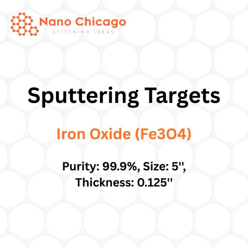
Iron Oxide (Fe3O4) Sputtering Targets
Technical Specifications
| Property | Value |
|---|---|
| Purity | 99.9% |
| Size | 7” |
| Thickness | 0.250” |
Overview
Sputtering is a proven technology used to deposit thin films from a wide range of materials onto various substrate shapes and sizes. The process using sputtering targets is highly repeatable and can be scaled from small research and development projects to production batches involving medium to large substrate areas. Depending on the process parameters, chemical reactions may occur on the target surface, in-flight, or on the substrate. Although sputter deposition involves many parameters and can be complex, it provides experts with extensive control over film growth and microstructure.
Applications of Sputtering Targets
Sputtering targets are used for thin film deposition. This method involves eroding material from a “target” and depositing it onto a “substrate,” such as a silicon wafer.
Semiconductor sputtering targets are used for target etching when a high degree of etching anisotropy is required and selectivity is not a concern.
Sputtering targets are also utilized for analytical purposes by etching away the target material. One example is secondary ion mass spectrometry (SIMS), where the sample is sputtered at a constant rate. As the target material is sputtered, the concentration and identity of the emitted atoms are analyzed using mass spectrometry. This allows determination of the material’s composition and detection of extremely low impurity levels.
Sputtering targets also find application in space-related studies. Sputtering is one of the mechanisms of space weathering, a process that alters the physical and chemical properties of airless bodies such as asteroids and the Moon.