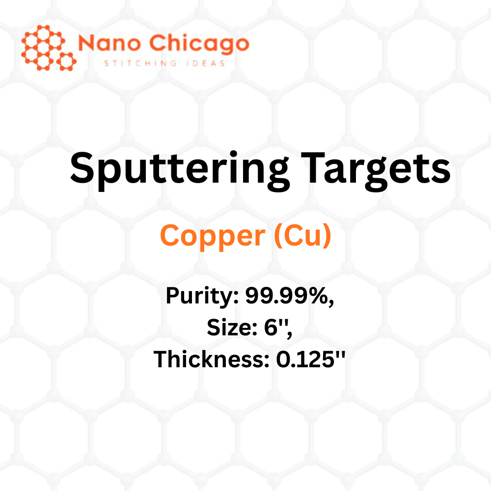
Copper (Cu) Sputtering Targets
| Section | Details |
|---|---|
| Product Name | Copper (Cu) Sputtering Targets |
| Purity | 99.99% |
| Size | 6” |
| Thickness | 0.125” |
| Process Overview | Sputtering is a proven technology capable of depositing thin films from a wide variety of materials onto diverse substrate shapes and sizes. The process with sputter targets is repeatable and can be scaled from small R&D projects. Targets can be adapted to production batches involving medium to large substrate areas. Chemical reactions can occur on the target surface, in-flight, or on the substrate depending on process parameters. The many parameters make sputter deposition complex but allow precise control over growth and microstructure. |
| Applications of Sputtering Targets | Sputtering targets are used for film deposition, involving erosion from a “target” onto a “substrate” like a silicon wafer. Semiconductor sputtering targets are used for etching when high anisotropy is needed. They are also used for analysis, such as in secondary ion spectroscopy (SIMS), where sputtered atoms are measured to determine target composition and detect extremely low impurities. Sputtering targets are applied in space weathering, altering physical and chemical properties of airless bodies like asteroids and the Moon. |