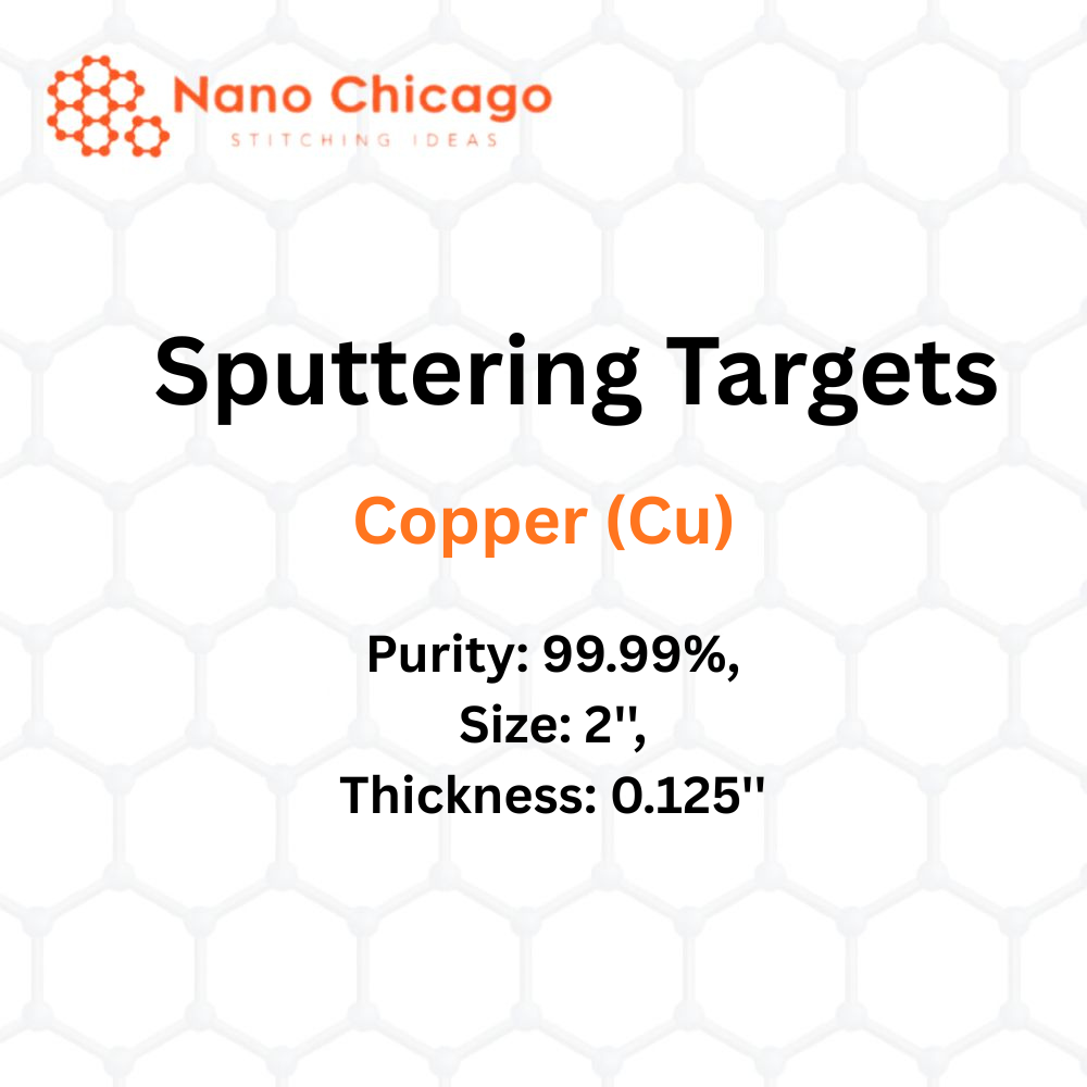
Copper (Cu) Sputtering Targets (2” × 0.125”, 99.99% purity):
| Section | Details |
|---|---|
| Product Name | Copper (Cu) Sputtering Targets |
| Purity | 99.99% |
| Size | 2” |
| Thickness | 0.125” |
| Process Overview | Sputtering enables deposition of thin films onto various substrate shapes and sizes. The process is repeatable and scalable from R&D to medium/large production batches. Chemical reactions may occur on the target surface, during flight, or on the substrate. Numerous adjustable parameters give experts control over film growth and microstructure. |
| Applications | • Thin Film Deposition: Erodes material from a target onto substrates like silicon wafers. • Semiconductor Etching: Used where high anisotropy is needed and selectivity is less critical. • Analytical Uses: In SIMS, the target is sputtered at a constant rate to measure composition and detect trace impurities via mass spectrometry. • Space Science: Sputtering contributes to space weathering, altering the physical and chemical properties of airless bodies such as asteroids and the Moon. |