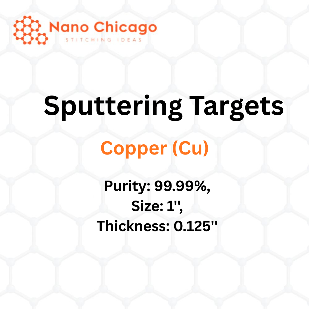
Copper (Cu) Sputtering Target — Product Specifications
| Property | Details |
|---|---|
| Material | Copper (Cu) |
| Purity | 99.99% |
| Size | 1” |
| Thickness | 0.125” |
| Description | Sputtering provides reliable thin-film deposition across various substrate shapes and sizes. The process is repeatable, scalable from R&D to large production, and allows precise control over film growth and microstructure. Chemical reactions may occur on the target surface, in-flight, or on the substrate depending on process parameters. |
Applications of Sputtering Targets
| Application Area | Explanation |
|---|---|
| Film Deposition | Material is eroded from the target and deposited onto a substrate (e.g., silicon wafer). |
| Semiconductor Etching | Used for sputter etching where high etching anisotropy is required and selectivity is less important. |
| Analytical Techniques (SIMS) | Used for controlled sputtering during Secondary Ion Mass Spectrometry to measure composition and detect trace impurities. |
| Space Science | Contributes to space weathering processes that modify the physical and chemical properties of airless bodies like the Moon and asteroids. |