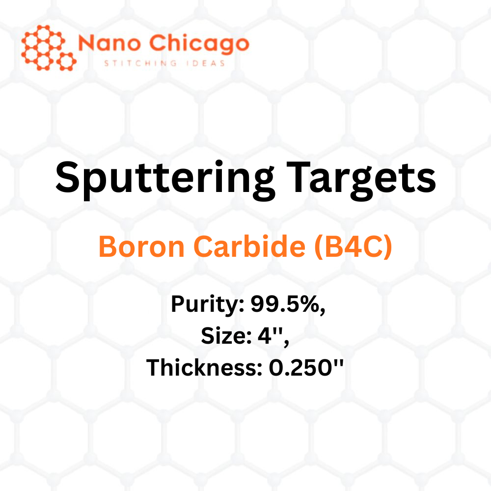
Boron Carbide (B4C) Sputtering Targets
Purity: 99.5%, Size: 4”, Thickness: 0.250”
Sputtering is a well-established technique capable of depositing thin films from a wide range of materials onto various substrate shapes and sizes.
The process using sputter targets is repeatable and can be scaled from small research and development projects to larger production needs. The process
with sputter targets can be adapted to production batches involving medium to large substrate areas. Chemical reactions may occur on the target surface,
in-flight, or on the substrate, depending on the process parameters. Although many parameters make sputter deposition complex, they also provide experts
with extensive control over growth and microstructure.
Applications of Sputtering Targets
Sputtering targets are used for film deposition. The deposition produced by sputter targets is a method of forming thin films by sputtering, which
involves eroding material from a “target” onto a “substrate,” such as a silicon wafer.
Semiconductor sputtering targets are used to etch the target. Sputter etching is selected when a high degree of etching anisotropy is required and
selectivity is not a key concern.
Sputter targets are also used for analytical purposes by etching away target material. One example occurs in secondary ion spectroscopy (SIMS), where
the target sample is sputtered at a constant rate. As the target is sputtered, the concentration and identity of ejected atoms are analyzed using mass
spectrometry. With the help of the sputtering target, the composition of the target material can be determined, and even extremely low impurity
concentrations can be detected.
Sputtering targets also have applications in space. Sputtering is one of the mechanisms of space weathering, a process that alters the physical and
chemical properties of airless bodies such as asteroids and the Moon.
Boron Nitride Overview
Boron nitride is a heat-resistant and chemically stable refractory compound composed of boron and nitrogen with the chemical formula BN. It exists in
several crystalline forms that are isoelectronic to similarly structured carbon lattices. The hexagonal form, which corresponds to graphite, is the most
stable and softest among BN polymorphs and is therefore used as a lubricant and as an additive in cosmetic products. The cubic form, known as c-BN, is
analogous to diamond. Although softer than diamond, it offers superior thermal and chemical stability. Due to its exceptional stability, boron nitride
ceramics are traditionally used in high-temperature equipment.
Cubic Boron Nitride in Coatings
Cubic boron nitride (c-BN) has become an important coating material for cutting tool applications due to its excellent mechanical and chemical
properties. Key properties of boron nitride include high hardness, a low friction coefficient, strong thermal conductivity, high electrical resistivity,
exceptional wear resistance, and chemical inertness at elevated temperatures. Boron nitride is the hardest material after diamond. Furthermore, it
surpasses diamond in chemical stability against oxygen and ferrous materials at high temperatures.
BN Polymorphs in Coatings
Boron nitride is primarily found in two polymorphs in coating applications: hexagonal boron nitride (h-BN) and cubic boron nitride (c-BN).
Hexagonal boron nitride is known for being soft, having a low friction coefficient, offering lubrication at both low and high temperatures, and being
electrically insulating and thermally conductive. It is widely used as a solid lubricant in metal forming dies and high-temperature forming processes
in various environments.
In contrast, the cubic phase offers high hardness and other extreme properties, making c-BN a preferred coating material for cutting tools. Due to these
advantages, the use of cubic boron nitride in applications such as dry cutting, high-speed machining, and cutting hard materials has increased in recent
years. Sintered cubic boron nitride cutting tools are already widely used in the market. However, their main drawbacks include high cost, low ductility,
and difficulty in forming them into different cutting tool geometries.
As a result, demand for thin or thick film deposition of BN—both for cutting applications and for protective coatings, optical coatings, and electrical
insulating layers—has grown rapidly. Many researchers are working to synthesize boron nitride coatings in the cubic phase. Among available coating
methods, the sputtering technique—a physical vapor deposition (PVD) process—stands out due to its lower coating temperature, ability to deposit thin
coatings, and suitability for coating sharp edges and complex shapes.