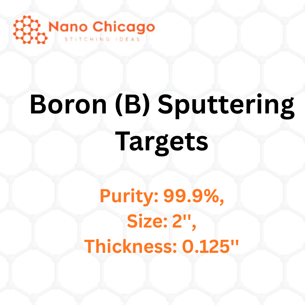
Boron (B) Sputtering Targets, 2” × 0.125”:
| Property | Specification |
|---|---|
| Product Name | Boron (B) Sputtering Targets |
| Purity | 99.9% |
| Size | 2” |
| Thickness | 0.125” |
| Description | Sputtering deposits thin films on diverse substrates. The process is repeatable, scalable from R&D to medium/large-area production, and allows precise control over growth and microstructure. Reactions can occur on the target, in-flight, or on the substrate depending on process parameters. |
| Applications of Sputtering Targets | – Thin-film deposition on substrates such as silicon wafers – Semiconductor sputter-etching requiring high anisotropy – Analytical etching (e.g., SIMS) to measure trace impurities – Space applications, studying weathering on airless bodies such as asteroids and the Moon – Ion implantation and ion-beam doping of semiconductors – Boron-containing coatings (e.g., boron nitride) for high hardness, toughness, corrosion and wear resistance – Trench filling in particle detectors and surface modification via ion implantation |