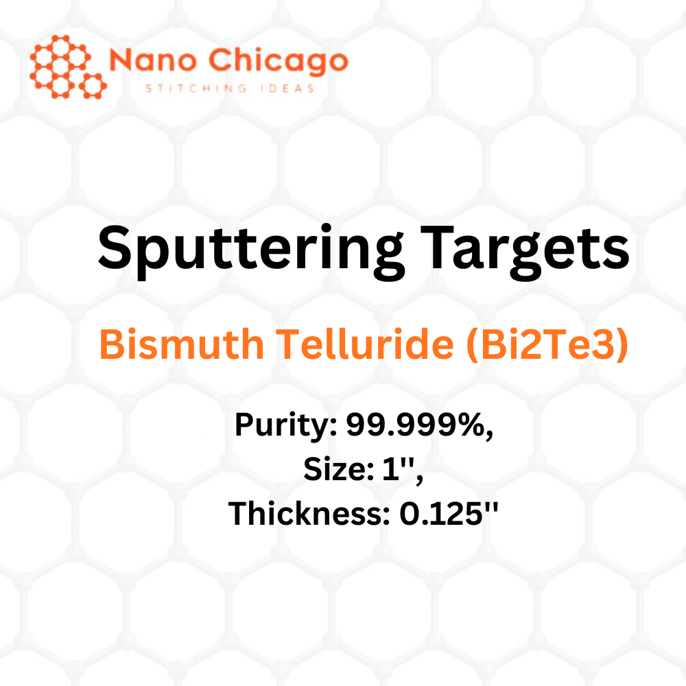
Bismuth Telluride (Bi₂Te₃) Sputtering Targets
Purity: 99.999% Size: 1” Thickness: 0.125”
Sputtering is a proven method for depositing thin films from a variety of materials onto substrates of different shapes and sizes. The process is highly repeatable and scalable, suitable for both research and medium-to-large production batches. Depending on parameters, chemical reactions may occur on the target surface, in-flight, or on the substrate, allowing precise control over film growth and microstructure.
Applications of Sputtering Targets
-
Thin Film Deposition: Erodes material from the target to deposit onto substrates such as silicon wafers.
-
Semiconductor Etching: Ideal for applications requiring high etching anisotropy without selectivity concerns.
-
Analytical Techniques: Secondary ion mass spectrometry (SIMS) uses sputtering to analyze target composition and detect trace impurities.
-
Space Applications: Contributes to space weathering, altering physical and chemical properties of airless bodies like asteroids and the Moon.
Bismuth Telluride (Bi₂Te₃) Properties and Uses
Bismuth telluride is a gray semiconductor compound of bismuth and tellurium. Alloyed with antimony or selenium, it becomes an efficient thermoelectric material for refrigeration and portable power generation. Bi₂Te₃ is also a topological insulator, showing thickness-dependent physical properties.
-
Thermoelectric Devices: Commonly used in bulk devices operating near ambient temperature.
-
Thin Film Applications: Nanostructured Bi₂Te₃ thin films are used in micro-coolers for thermal management and flexible micro-power generators.
-
Enhanced Performance: Advances in nanotechnology and well-ordered thin film structures significantly improve thermoelectric efficiency over bulk materials.
-
Research Considerations: Composition, microstructure, morphology, thickness, stress-strain, and substrate conditions all influence thin film thermoelectric properties.