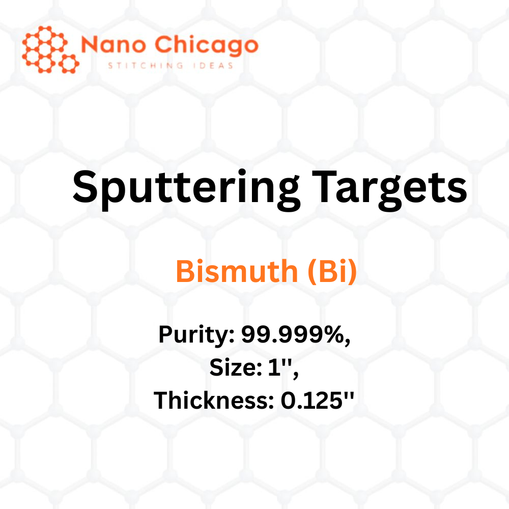
Bismuth (Bi) Sputtering Targets
Purity: 99.999% Size: 1” Thickness: 0.125”
Overview:
Bismuth sputtering targets are ideal for depositing high-quality thin films on diverse substrate shapes and sizes. The sputtering process is repeatable and scalable, suitable for both R&D projects and medium to large production batches. Chemical reactions can occur on the target surface, in-flight, or on the substrate depending on process parameters, offering precise control over film growth and microstructure.
Applications:
-
Thin film deposition on substrates like silicon wafers.
-
Semiconductor etching where high anisotropy is required.
-
Analytical techniques such as secondary ion mass spectrometry (SIMS) for composition analysis and impurity detection.
-
Space applications, simulating space weathering effects on airless bodies like asteroids or the Moon.
Material Properties:
Bismuth is a silvery-pink brittle metal, stable in air and water. It has low thermal and electrical conductivity but is widely used in fusible alloys, low-melting-point applications, gamma-ray absorption filters, thermoelectric devices, magneto-resistance applications, and heavy-metal detection electrodes. Thin Bi films (≈30 nm) can transform into semiconductors and can be deposited via RF/DC sputtering, laser pulsed deposition, or thermal evaporation. Film density and morphology can be finely tuned using PVD techniques, including positive pulsing during DC sputtering.