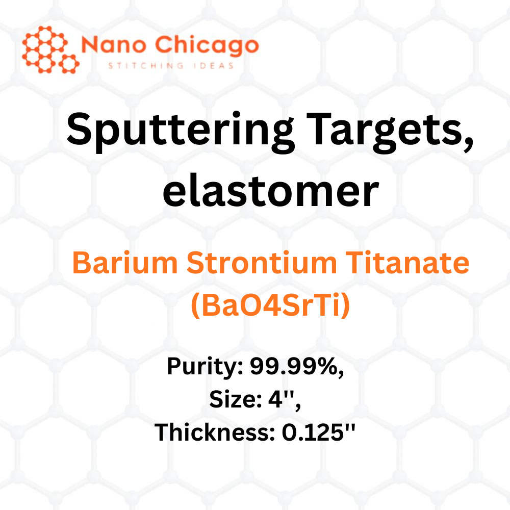
Barium Strontium Titanate (BaO4SrTi) Sputtering Targets, Elastomer
Purity: 99.99% | Size: 4” | Thickness: 0.125”
Sputtering is a well-established technology capable of depositing thin films onto a wide variety of materials and diverse substrate shapes. The process using sputter targets is repeatable and can be scaled from small research and development projects to production batches involving medium to large substrate areas. Chemical reactions may occur on the target surface, in-flight, or on the substrate depending on the process parameters. These variables make sputter deposition a complex process, but they provide experts with precise control over film growth and microstructure.
Applications of Sputtering Targets:
-
Sputtering targets are primarily used for film deposition. The process involves eroding material from a “target” source onto a “substrate,” such as a silicon wafer.
-
Semiconductor sputtering targets are used for etching, especially when a high degree of anisotropy is required and selectivity is not a concern.
-
Sputter targets are also used in analytical applications, such as secondary ion spectroscopy (SIMS), where the target sample is sputtered at a constant rate. During this process, the concentration and identity of sputtered atoms are measured using mass spectrometry, allowing determination of the target material’s composition and detection of extremely low concentrations of impurities.
Sputtering targets also have applications in space. Sputtering contributes to space weathering, a process that alters the physical and chemical properties of airless bodies, such as asteroids and the Moon.
Barium strontium titanate (BST) is a solid solution of barium titanate (BaTiO3) and strontium titanate (SrTiO3). Thin films of BST obtained through sputtering exhibit excellent dielectric properties, making them ideal for ferroelectric thin-film devices. Over the last decade, BST-based devices have been widely used in tunable microwave applications such as delay lines, resonators, phase shifters, and varactors.
BST thin films are promising due to their high dielectric constant, tunability, and low dielectric loss. Dielectric-tunable properties of BST films deposited by various techniques have been studied extensively, considering factors such as oxygen vacancies, film thickness, grain size, Ba/Sr ratio, and more. Researchers have also investigated doping concentrations, high-temperature annealing, and multilayer structures to achieve enhanced tunability and reduced dielectric loss.