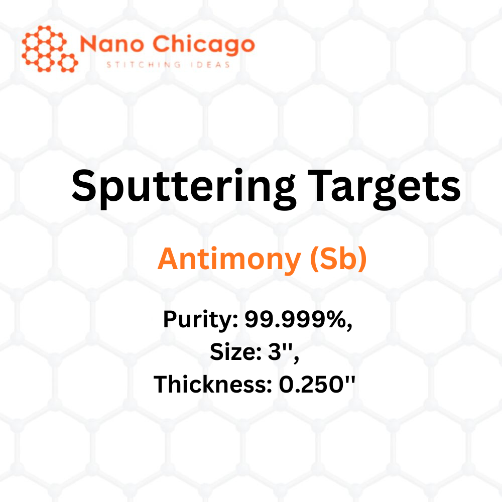
Antimony (Sb) Sputtering Targets
Purity: 99.999% | Size: 3” | Thickness: 0.250”
Antimony sputtering targets are designed for precise thin-film deposition on a variety of substrate shapes and sizes. The sputtering process is reliable and scalable, supporting both research and large-scale production. Reactions can occur on the target surface, in-flight, or on the substrate depending on process parameters, offering precise control over film growth and microstructure.
Applications:
-
Thin-film deposition on substrates such as silicon wafers.
-
Semiconductor etching requiring high anisotropy.
-
Material analysis, including SIMS, for trace impurity detection.
-
Space applications: contributes to space weathering on airless bodies like asteroids and the Moon.
-
Fire-retardant coatings.
-
Optoelectronic devices: LEDs, laser diodes, photodiodes, and solar cells.
-
Transparent conductive films using antimony alloys (e.g., indium-antimony oxide).
About Antimony (Sb):
Antimony (atomic number 51) is a bluish-white metalloid in Group 15, with chemical properties similar to arsenic. It is used as a dopant in n-type silicon wafers for diodes, infrared detectors, and Hall-effect devices. Antimony forms alloys with elements like tin and indium, enabling applications in transparent conductive films, flexible coatings, and optoelectronic devices.

