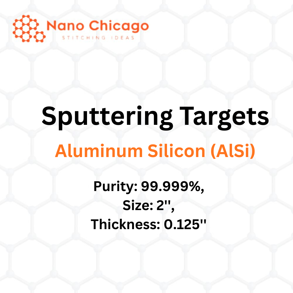
Aluminum Silicon (AlSi) Sputtering Targets
Purity: 99.999% Size: 2” Thickness: 0.125”
Aluminum Silicon (AlSi) sputtering targets are ideal for precise thin-film deposition on diverse substrate shapes and sizes. The process is highly repeatable and scalable, suitable for both research and medium-to-large production batches. Depending on the process parameters, chemical reactions can occur on the target surface, in-flight, or on the substrate, allowing experts full control over film growth and microstructure.
Applications of Sputtering Targets
-
Thin-Film Deposition:
Erodes material from the target onto substrates, such as silicon wafers, to form uniform thin films. -
Semiconductor Etching:
Used for sputter etching when high anisotropy is needed and selectivity is less critical. -
Material Analysis (SIMS):
Supports secondary ion mass spectrometry for determining target composition and detecting trace impurities. -
Space Applications:
Contributes to space weathering, modifying the physical and chemical properties of airless bodies like asteroids and the Moon.