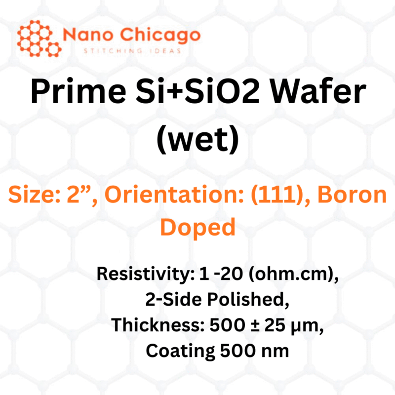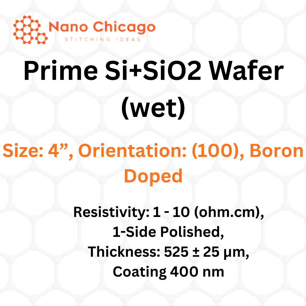
Prime Si+SiO2 Wafer (Wet)
| Parameter | Specification |
|---|---|
| Size | 4” |
| Orientation | (100) |
| Doping | Boron |
| Polished | One Side |
| Thickness | 525 ± 25 μm |
| Coating | 400 nm |
Silicon dioxide wafers, also referred to as thermal oxide wafers, are produced at elevated temperatures.
Thermal oxide is typically grown in a horizontal tube furnace at temperatures ranging from 900 °C to 1200 °C.
Unlike CVD-deposited oxide layers, thermal oxide is a “grown” oxide layer, offering higher uniformity and greater dielectric strength, making it an excellent insulating layer.
In most silicon-based devices, the thermal oxide layer is crucial for passivating the silicon surface, acting as a doping barrier and surface dielectric.
This method provides excellent thickness uniformity and purity, making it the preferred technique for producing high-quality thin silicon oxide layers.
Thicker oxide layers are generally produced through wet oxidation, where the growth rate is significantly increased.