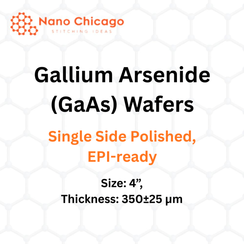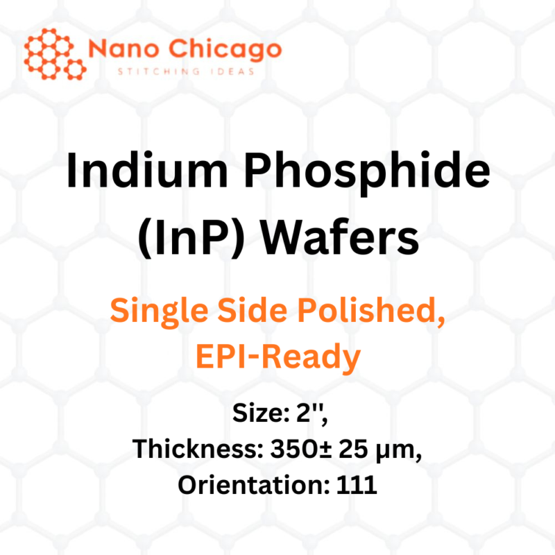
Indium Phosphide (InP) Wafers
Size: 4”, Thickness: 625± 25 μm, Orientation: 100
Technical Properties
| Property | Value |
|---|---|
| Size (inch) | 4” |
| Thickness (μm) | 625± 25 |
| Dopant | Sulphur (N type) |
| Polished | Single Side |
| Mobility | (1.5-3.5)E3 |
| Orientation | 100 |
| EPD | ≤5000 |
| Growth method | VGF |
| OF Length | 32.5±2 |
| IF Length | 18±1 |
Fields of Application for Indium Phosphide (InP)
Indium phosphide (InP) is a binary semiconductor composed of indium and phosphorus.
Indium phosphide (InP) began development in the early 1980s.
Indium phosphide (InP), used in high-power and high-frequency electronics, exhibits superior electron velocity. Its direct bandgap, unlike many semiconductors, makes it highly suitable for optoelectronics and laser diodes. Indium phosphide (InP) is crucial for generating laser signals and converting them back to electronic form.
Indium Phosphide (InP) belongs to a group of materials commonly known as III-V Semiconductors.
InP is employed in high-power and high-frequency electronics and demonstrates superior electron velocity compared to semiconductors such as Silicon and Gallium Arsenide.
Indium Phosphide has a face-centered cubic crystal structure, similar to GaAs and most III-V semiconductors.
InP wafers must be prepared prior to device fabrication. All III-V wafers are lapped to remove surface damage from slicing. Wafers are then Chemically Mechanically Polished/Planarized (CMP) for the final material removal stage, achieving super-flat, mirror-like surfaces with atomic-scale roughness. The wafer is then ready for device fabrication.
Indium phosphide (InP) is used in modulators.
Indium phosphide (InP) is used in photo-detectors.
Indium phosphide (InP) is used in LEDs.
Indium phosphide (InP) is used in fiber communications components.
Indium phosphide (InP) is used in semiconductor optical amplifiers.
Applications
Carbon nanotubes doped with metallic nanopowders provide significant enhancements in both electrical and mechanical performance. These improvements include increased hardness, tensile strength, specific strength, and elastic modulus. As a result, these materials are widely utilized across various fields. Some of these applications include: 1-drug delivery, 2-biosensors, 3-CNT composites, 4-catalysis, 5-nanoprobes, 6-hydrogen storage, 7-lithium batteries, 8-gas-discharge tubes, 9-flat panel displays, 10-supercapacitors, 11-transistors, 12-solar cells, 13-photoluminescence, 14-templates.