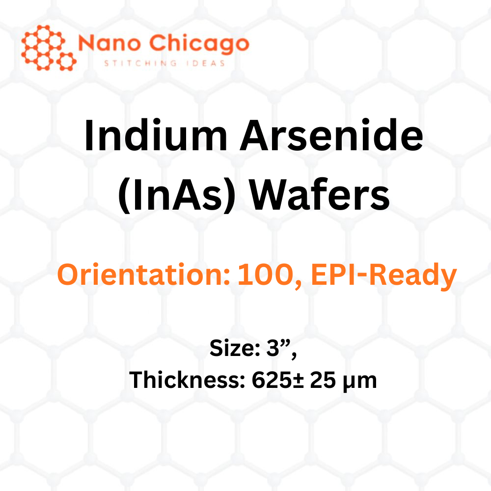
Indium Arsenide (InAs) Wafer
Technical Properties
| Parameter | Specification |
|---|---|
| Quality | EPI-Ready |
| Size | 3” |
| Thickness | 625 ± 25 μm |
| Polished | Single Side |
| Dopant | Zinc/Sulphur (Zn/S, N-Type) |
| Orientation | (100) |
| Mobility | 6000–20,000 |
| EPD | ≤ 50,000 |
| Growth Method | VGF |
| OF Length | 22 ± 2 |
| IF Length | 11 ± 1 |
Applications of Indium Arsenide (InAs) Wafer
Indium arsenide (InAs) is a compound semiconductor made from indium and arsenic. Like gallium arsenide (GaAs), it is a direct bandgap material with several unique electronic and optical properties.
Key characteristics include:
-
High electron mobility
-
Narrow bandgap
-
Strong Photo-Dember emission
These properties make InAs wafers widely used as terahertz radiation sources and suitable for high-performance optoelectronic devices.
Common Applications
-
Infrared Detectors (1–3.8 μm range)
Used in photovoltaic photodiodes; effective at room temperature and even better when cryogenically cooled. -
Diode Lasers
InAs serves as an important material in fabricating diode laser structures. -
Terahertz Sources
Due to strong Photo-Dember effect. -
Optical and Photonic Devices
Including specialized military specifications, food inspection systems, and optical-grade detector applications.
Indium arsenide wafers are available in n-type, p-type, or semi-insulating variants and can be produced in different orientations depending on device requirements.
InAs appears as grey cubic crystals and has a melting point of 942°C, underscoring its suitability for advanced semiconductor applications.