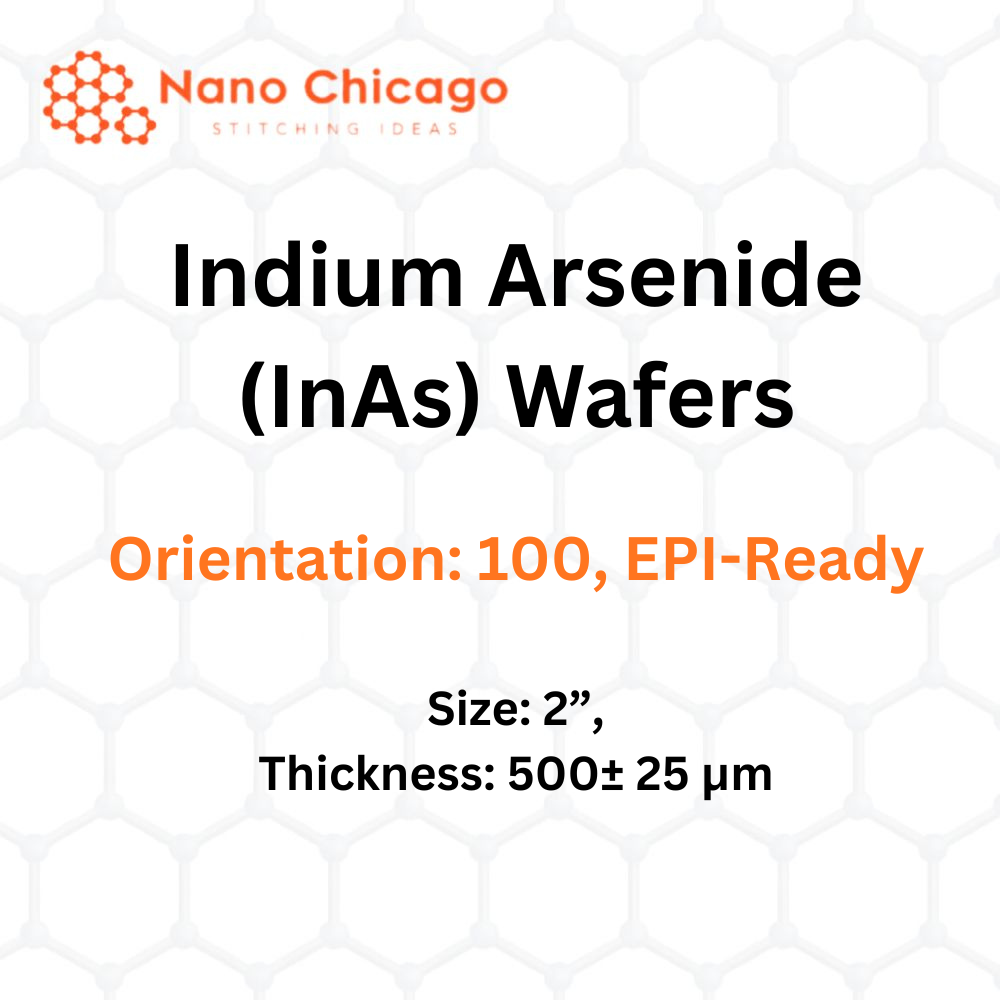
Indium Arsenide (InAs) Wafers
Size: 2”, Thickness: 500± 25 μm, Orientation: 100
Technical Properties
| Quality | EPI-Ready |
|---|---|
| Size (inch) | 2” |
| Thickness (μm) | 500± 25 |
| Polished | Single Side |
| Dopant | Zinc/Sulphur (Zn/S, N Type) |
| Orientation | 100 |
| Mobility | 6000-20000 |
| EPD | ≤50000 |
| Growth method | VGF |
| OF Length | 16±2 |
| IF Length | 8±1 |
Fields of Application for Indium Arsenide (InAs) Wafer
Indium arsenide (InAs) is a compound of indium and arsenic, and is a semiconductor material. It is similar to gallium arsenide and is a direct bandgap material.
Due to its high electron mobility, narrow energy bandgap, and strong Photo-Dember emission, indium arsenide (InAs) wafers are widely used as terahertz radiation sources.
They can be supplied in n type, p type, or semi-insulating forms with various orientations.
Indium arsenide (InAs) appears as grey cubic crystals with a melting point of 942 °C.
It is commonly used in the construction of infrared detectors, covering a wavelength range of 1–3.8 µm. These detectors are typically photovoltaic photodiodes. Cryogenically cooled detectors exhibit lower noise, but InAs detectors are also suitable for higher-power applications at room temperature.
Indium arsenide is additionally used in the fabrication of diode lasers.
Some specific applications include: Indium arsenide (InAs) wafer is used for infrared detectors, mil specs, food industry, and optical-grade devices. Diode lasers are also manufactured using indium arsenide (InAs) wafers.