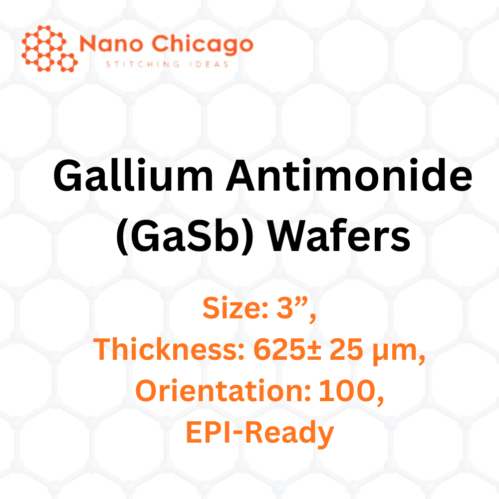
Gallium Antimonide (GaSb) Wafers
Size: 3”, Thickness: 625 ± 25 μm, Orientation: 100
Technical Properties:
| Quality | EPI-Ready |
|---|---|
| Size (inch) | 3” |
| Thickness (μm) | 625 ± 25 |
| Polished | Single Side |
| Dopant | Tellurium (N type) |
| Orientation | 100 |
| Mobility | 2000-3500 |
| EPD | ≤2000 |
| Growth method | VGF |
| OF Length | 22 ± 2 |
| IF Length | 11 ± 1 |
Fields of Application for Gallium Antimonide (GaSb)
The intermetallic compound gallium antimonide (GaSb) was first prepared in 1926 by Victor Goldschmidt.
Gallium antimonide (GaSb) is a semiconductor composed of gallium and antimony, classified as a group III-V compound. It is supplied in polished wafer form. GaSb wafers are produced from polycrystalline ingots using the Czochralski method to obtain single crystals with high purity.
Polished GaSb wafers offer very high orientation accuracy. The thickness and orientation of these wafers can be modified with additives. The Czochralski method ensures the growth of pure gallium and antimony elements. The naturally low-defect structure of GaSb makes it ideal for epitaxial growth. Wafers are available in single-side or double-side polished and cut forms.
Gallium antimonide (GaSb) is used for infrared detectors, infrared LEDs, transistors, lasers, and thermophotovoltaic systems.