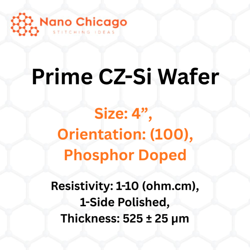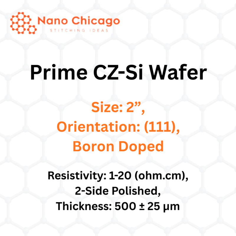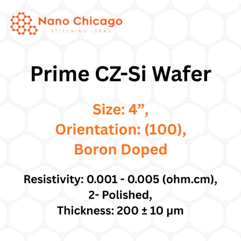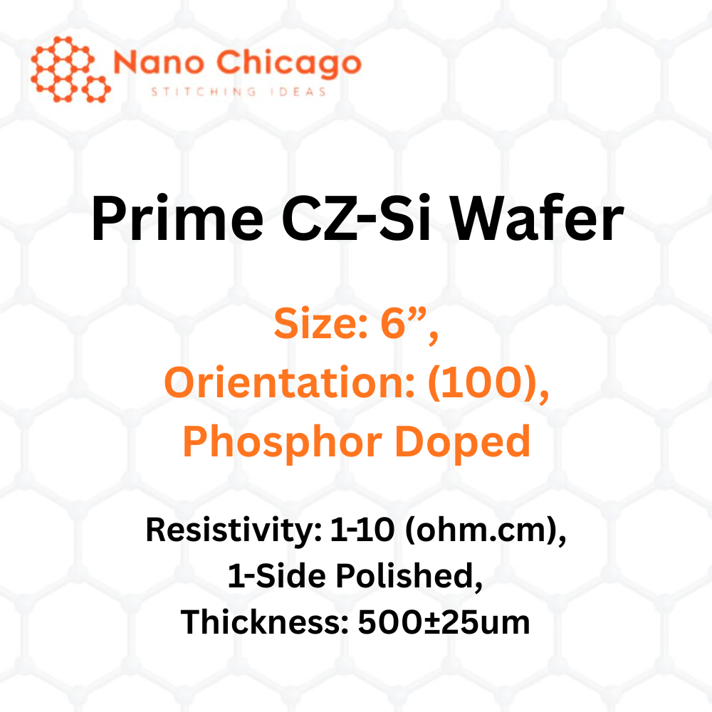
Prime CZ-Si Wafer
Size: 6”, Orientation: (100), Phosphor Doped, 1-Side Polished, Thickness: 500±25um
Technical Properties:
| Quality | Prime |
|---|---|
| Materials | CZ-Si |
| Size (inch) | 6” |
| Orientation | (100) |
| Coating | |
| Thickness (μm) | 500±25um |
| Doping | Phosphor |
| Resistivity (ohm.cm) | 1-10 |
| Polished | One Side |
Silicon is one of the most abundant elements in the Earth’s crust. The primary use of silicon wafers is in electronics and advanced technology sectors. These wafers feature extremely flat, mirror-like surfaces and are produced using the Czochralski method to achieve high purity. Depending on application requirements, silicon wafers may be doped with various materials to modify their purity and electronic behavior. The type and concentration of dopants—such as gallium, indium, boron, or nitrogen—significantly influence electrical properties.
Silicon wafers play a critical role in semiconductors, microchips, integrated circuits, smartphones, computers, and other electronic systems. As the foundational platform for semiconductor devices, a wafer serves as a thin substrate upon which microelectronic components are built and integrated.