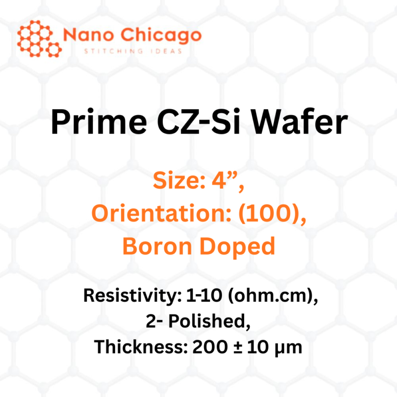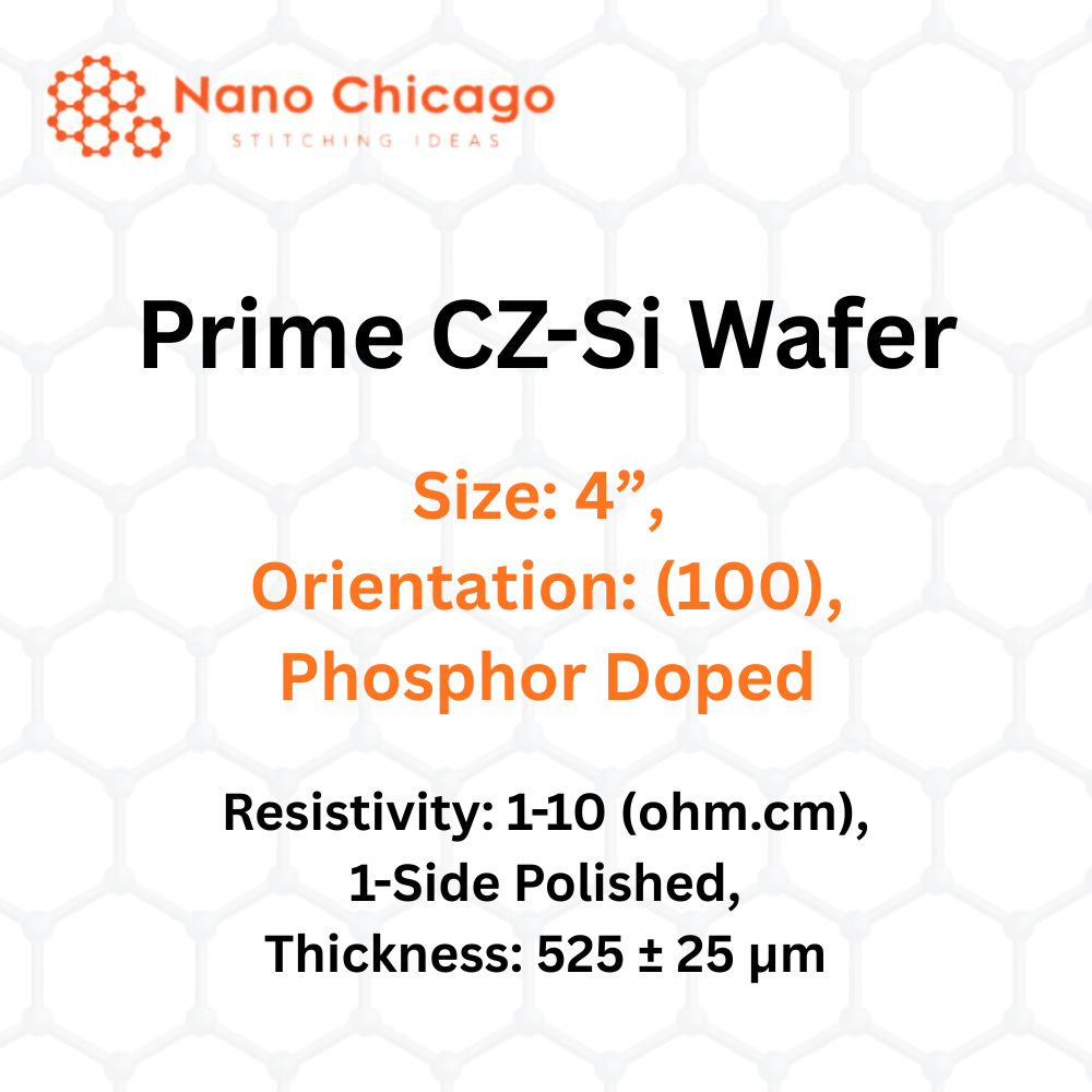
Prime CZ-Si Wafer
Size: 4”, Orientation: (100), Phosphor Doped, 1-Side Polished
Technical Properties:
| Quality | Prime |
|---|---|
| Materials | CZ-Si |
| Size (inch) | 4” |
| Orientation | (100) |
| Coating | |
| Thickness (μm) | 525 ± 25 |
| Doping | Phosphor |
| Resistivity (ohm.cm) | 1-10 |
| Polished | One Side |
Silicon is one of the most common elements in the Earth’s crust. The primary application of silicon wafers is in electronics and advanced technology. These wafers feature extremely flat, mirror-like surfaces and are produced using the Czochralski method to achieve high purity. Depending on the intended use, silicon wafers can be doped with various materials to adjust their purity and electronic characteristics. The type and concentration of dopants—such as gallium, indium, boron, and nitrogen—play a significant role in determining electronic performance.
Silicon wafers are essential components in semiconductors, microchips, integrated circuits, smartphones, computers, and other electronic devices. As the foundation for semiconductor components, a wafer serves as a thin substrate that supports microelectronic devices embedded on and above its surface.