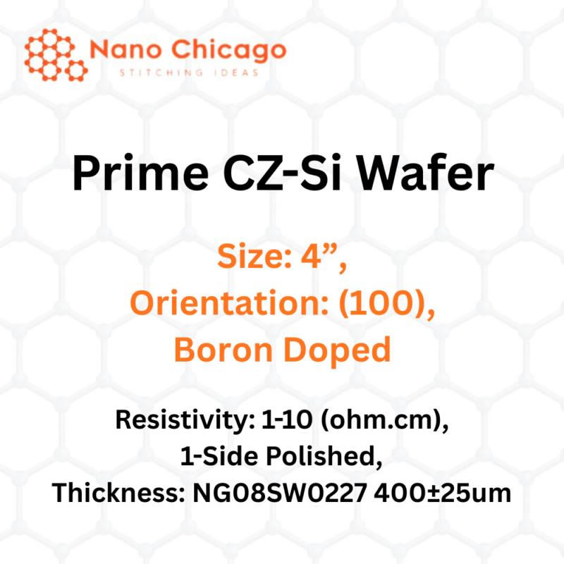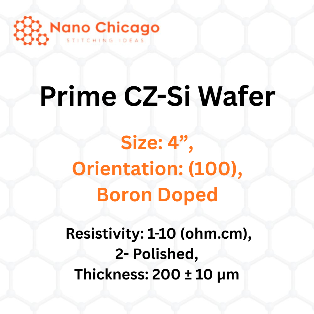
Prime CZ-Si Wafer
Size: 4”, Orientation: (100), Boron Doped, 2-Polished
Technical Properties:
| Quality | Prime |
|---|---|
| Materials | CZ-Si |
| Size (inch) | 4” |
| Orientation | (100) |
| Coating | |
| Thickness (μm) | 200 ± 10 |
| Doping | Boron |
| Resistivity (ohm.cm) | 1-10 |
| Polished | Double Side |
Silicon is one of the most common elements in the Earth’s crust. The primary use of silicon wafers lies in electronics and advanced technology. These wafers possess extremely flat, mirror-like surfaces and are manufactured using the Czochralski method to achieve exceptional purity. Depending on application requirements, silicon wafers can be doped with various materials to tailor their electronic characteristics. The type and concentration of dopants—such as gallium, indium, boron, and nitrogen—significantly influence electrical properties.
Silicon wafers are essential components in semiconductors, microchips, integrated circuits, smartphones, computers, and many other electronic devices. As the foundational platform for semiconductor components, a wafer serves as a thin substrate where microelectronic structures are formed both on and within its surface.