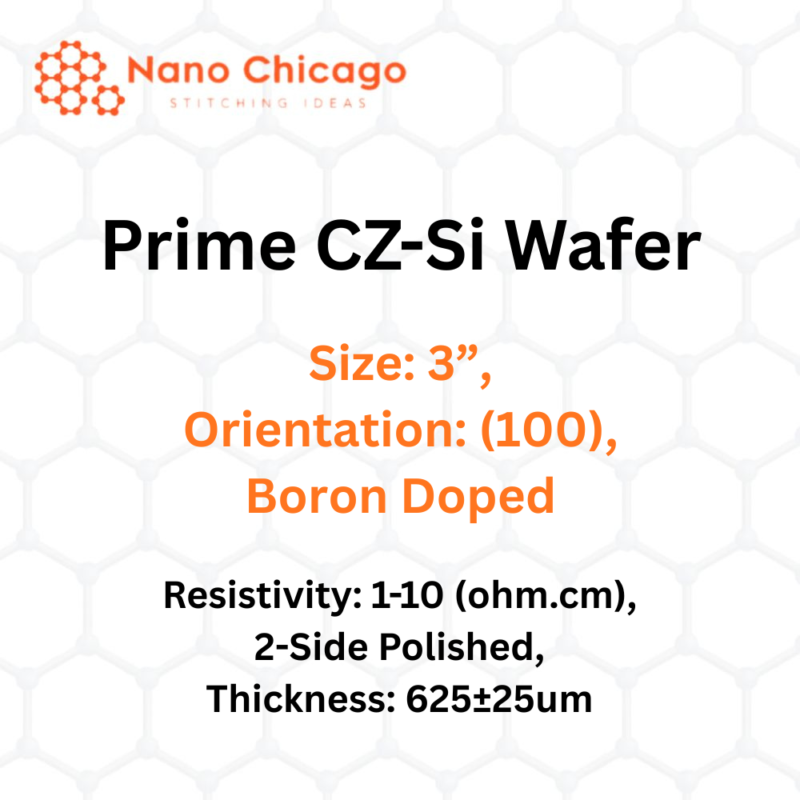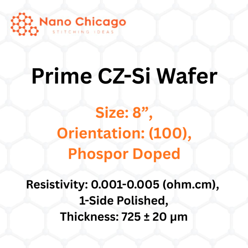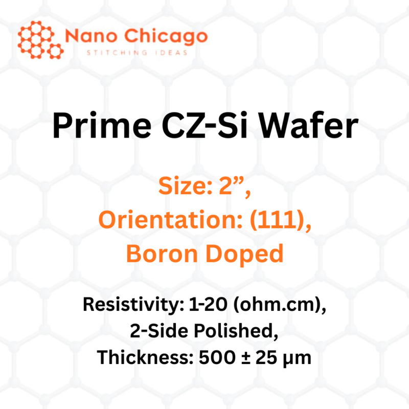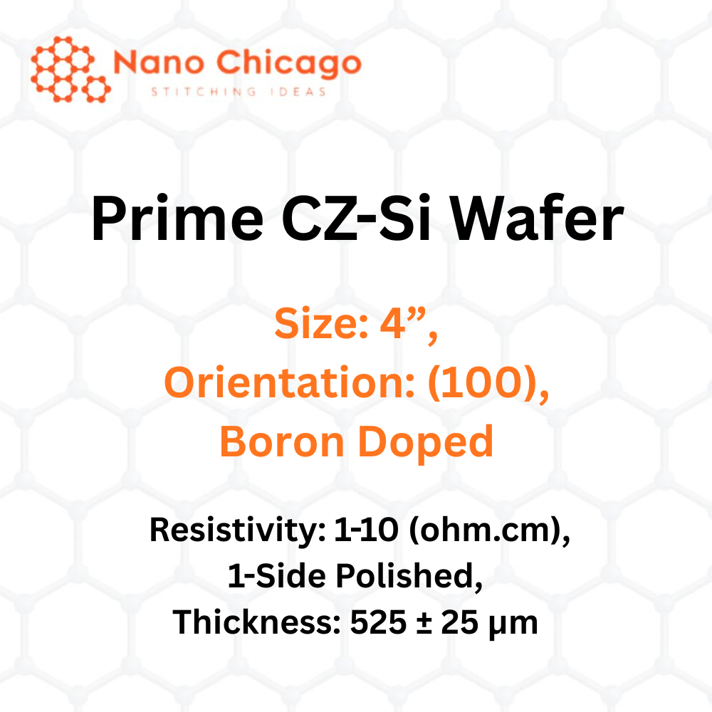
Prime CZ-Si Wafer
Size: 4”, Orientation: (100), Boron Doped, 1-Side Polished
Technical Properties:
| Quality | Prime |
|---|---|
| Materials | CZ-Si |
| Size (inch) | 4” |
| Orientation | (100) |
| Coating | |
| Thickness (μm) | 525 ± 25 |
| Doping | Boron |
| Resistivity (ohm.cm) | 1-10 |
| Polished | One Side |
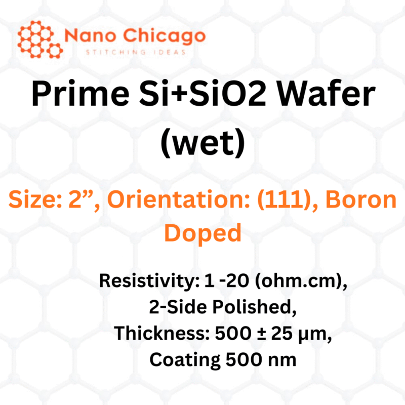
Silicon is one of the most common elements found in the Earth’s crust. The primary use of silicon wafers is in electronics and technology. These wafers have extremely flat, mirror-like surfaces and are produced using the Czochralski method to achieve maximum purity. Depending on the application, silicon wafers can be doped with various materials to adjust their purity and electronic characteristics. The amount and type of dopants significantly influence electrical performance. Gallium, indium, boron, and nitrogen are among the dopants commonly used during production.
Silicon wafers are essential components in semiconductors, microchips, integrated circuits, smartphones, computers, and many other devices. As the foundation of semiconductor technology, a wafer is a thin slice of semiconductor material that serves as the substrate for microelectronic components built on and above its surface.