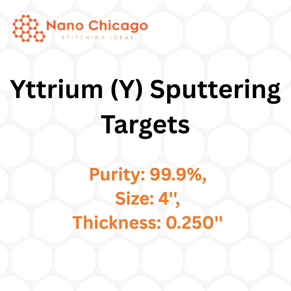
Product Table
| Property | Specification |
|---|---|
| Material | Yttrium (Y) |
| Purity | 99.9% |
| Size | 4” |
| Thickness | 0.250” |
| Form | Sputtering Target |
Description
Yttrium (Y) sputtering targets are ideal for depositing high-quality thin films on various substrate types. Sputtering ensures repeatable, scalable deposition with precise control over film microstructure. The process can be adapted for both small R&D applications and larger production batches, with reactions occurring on the target surface, in-flight, or on the substrate depending on parameters.
Applications
-
Thin-film deposition on substrates like silicon wafers
-
Semiconductor sputter etching for high anisotropy without selectivity concerns
-
Material analysis, such as SIMS, for detecting extremely low concentrations of impurities
-
Space research applications, including simulation of space weathering on asteroids and the Moon.