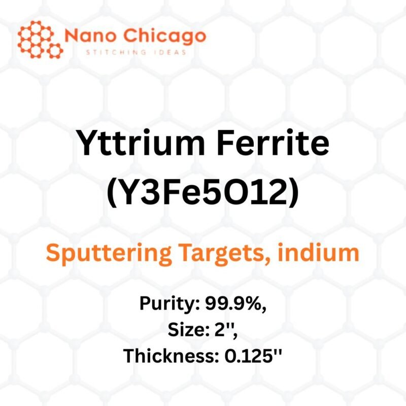
Product Table
| Property | Specification |
|---|---|
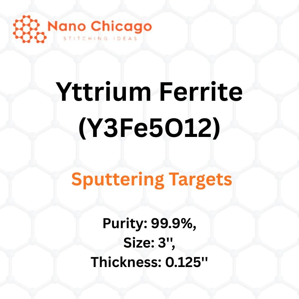
| Material | Yttrium Ferrite (Y₃Fe₅O₁₂) |
| Purity | 99.9% |
| Size | 3” |
| Thickness | 0.125” |
| Form | Sputtering Target |
Description
Yttrium Ferrite (Y₃Fe₅O₁₂) sputtering targets are used for thin-film deposition across a wide range of substrates and materials. Sputtering technology enables precise, repeatable film growth and can be scaled from small R&D applications to medium and large production environments. Depending on process conditions, chemical reactions may occur on the target surface, during particle transport, or at the substrate. Though complex, sputtering provides extensive control over film thickness, microstructure, and uniformity.
Applications
-
Thin Film Deposition: Material is sputtered from the target and deposited onto substrates such as silicon wafers.
-
Semiconductor Processing: Used in sputter etching where high anisotropy is required.
-
Material Analysis: Utilized in SIMS (Secondary Ion Mass Spectrometry) to determine composition and detect trace impurities by sputtering the sample surface.
-
Space Science: Sputtering is a natural phenomenon contributing to space weathering of airless planetary bodies like the Moon and asteroids.