Ytterbium Oxide (Yb₂O₃) Sputtering Targets — Product Table
| Category | Details |
|---|---|
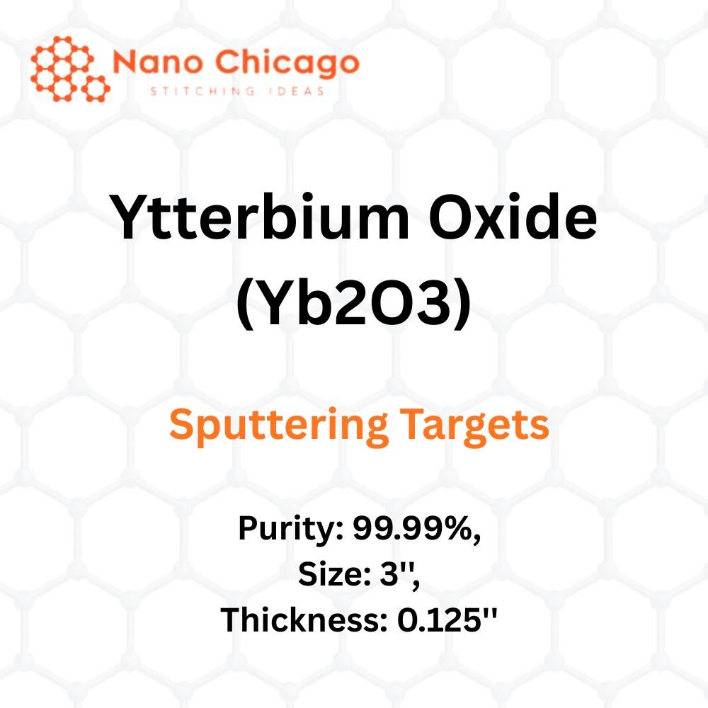
| Product Name | Ytterbium Oxide (Yb₂O₃) Sputtering Targets |
| Purity | 99.99% |
| Size | 3” |
| Thickness | 0.125” |
| Material | Ytterbium Oxide (Yb₂O₃) |
| Process Description | Sputtering is a repeatable, scalable thin-film deposition method capable of coating diverse substrates. Chemical reactions may occur on the target surface, in-flight, or on the substrate depending on process parameters. Provides controlled growth and microstructure formation. |
Applications
| Application Area | Description |
|---|---|
| Thin Film Deposition | Used to deposit thin films by sputtering, transferring material from the target to substrates such as silicon wafers. |
| Semiconductor Etching | Used for sputter etching when high anisotropy is required and selectivity is not a priority. |
| Material Analysis (SIMS) | Used to sputter material at a constant rate for impurity detection and compositional analysis through mass spectrometry. |
| Space Science | Plays a role in space weathering processes, altering physical and chemical properties of bodies like the Moon and asteroids. |