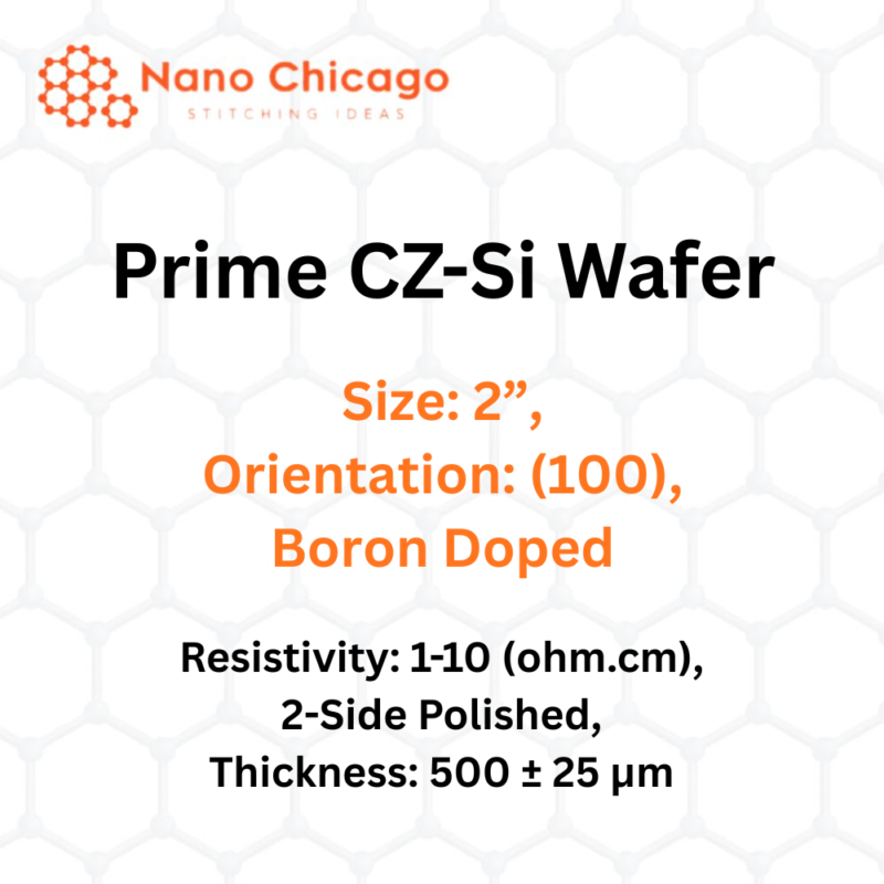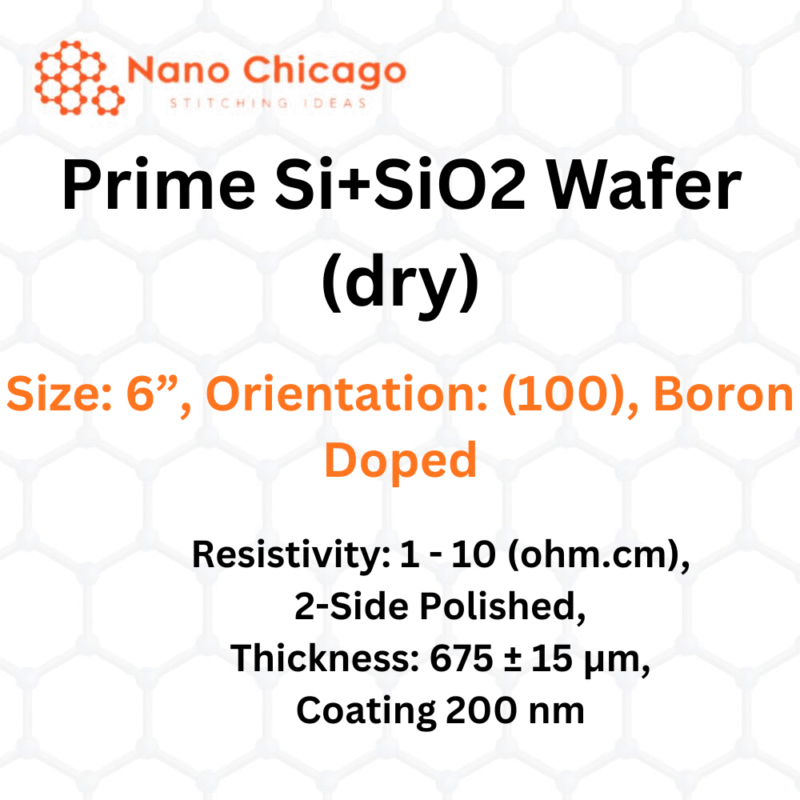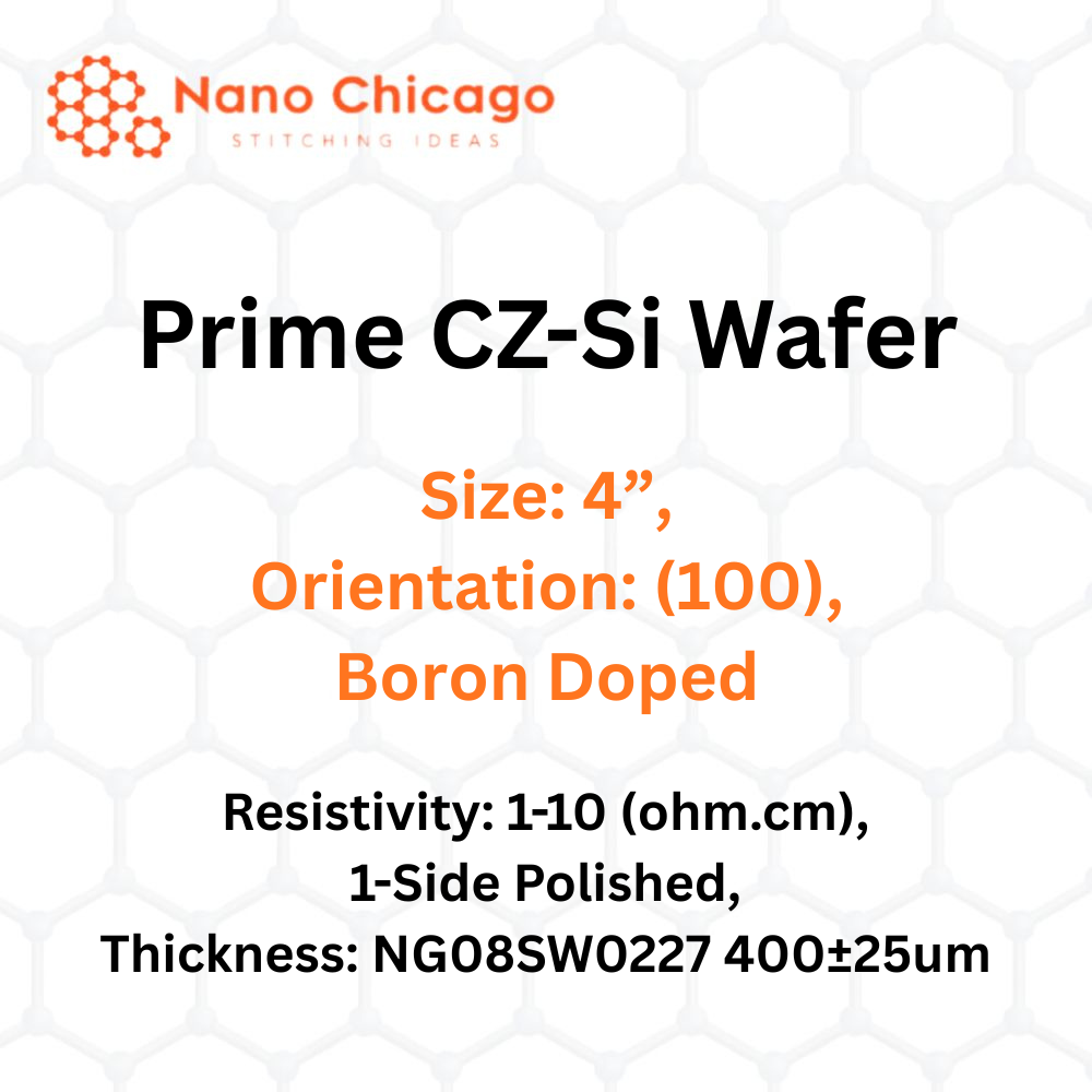
Prime CZ-Si Wafer
Size: 4”, Orientation: (100), Boron Doped, 1-Side Polished
Technical Properties:
| Quality | Prime |
|---|---|
| Materials | CZ-Si |
| Size (inch) | 4” |
| Orientation | (100) |
| Coating | |
| Thickness (μm) | 400±25um |
| Doping | Boron |
| Resistivity (ohm.cm) | 1-10 |
| Polished | One Side |
Silicon is one of the most abundant elements in the Earth’s crust. The primary use of silicon wafers lies in electronics and advanced technology applications. These wafers possess extremely flat, mirror-like surfaces and are produced using the Czochralski method to achieve the highest purity. According to specific application needs, silicon wafers can be doped with various materials to tailor their purity and electronic characteristics. The type and concentration of dopants—such as gallium, indium, boron, and nitrogen—significantly influence the material’s electronic behavior.
Silicon wafers are essential components in semiconductors, microchips, integrated circuits, smartphones, computers, and other electronic technologies. As the fundamental platform for semiconductor devices, a wafer serves as a thin substrate on which microelectronic components are built and integrated.