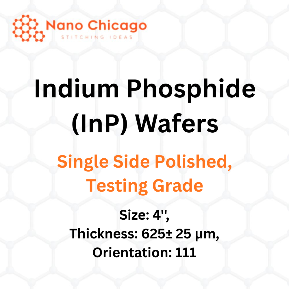
Indium Phosphide (InP) Wafers
Size: 4”, Thickness: 625± 25 μm, Orientation: 111
Technical Properties:
| Size (inch) | 4” |
|---|---|
| Thickness (μm) | 625± 25 |
| Dopant | Sulphur (N type) |
| Polished | Single Side |
| Mobility | (1.5-3.5)E3 |
| Orientation | 111 |
| EPD | ≤5000 |
| Growth method | VGF |
| OF Length | 32.5±2 |
| IF Length | 18±1 |
Fields of Application for Indium Phosphide (InP)
Indium phosphide (InP) is a binary semiconductor composed of indium and phosphorus.
Indium phosphide (InP) began development in the early 1980s. It is used in high power and high-frequency electronics and has superior electron velocity. Indium phosphide (InP) has a direct bandgap compared to many other semiconductors, making it ideal for optoelectronics and laser diodes. It is a crucial material for generating laser signals, as well as for detecting and converting those signals back to electronic form.
Indium phosphide (InP) belongs to the III-V semiconductor family.
InP is used in high power and high-frequency electronics and offers superior electron velocity compared to common semiconductors such as Silicon and Gallium Arsenide.
Indium phosphide has a face-centered cubic crystal structure, almost identical to that of GaAs and most III-V semiconductors.
InP wafers must be prepared prior to device fabrication. All III-V wafers are lapped to remove surface damage from slicing. Wafers are then chemically mechanically polished (CMP) to achieve super-flat, mirror-like surfaces with atomic-scale roughness, making them ready for device fabrication.
Indium phosphide (InP) is used in modulators.
Indium phosphide (InP) is used in photo-detectors.
Indium phosphide (InP) is used in LEDs.
Indium phosphide (InP) is used in fiber communications components.
Indium phosphide (InP) is used in semiconductor optical amplifiers.