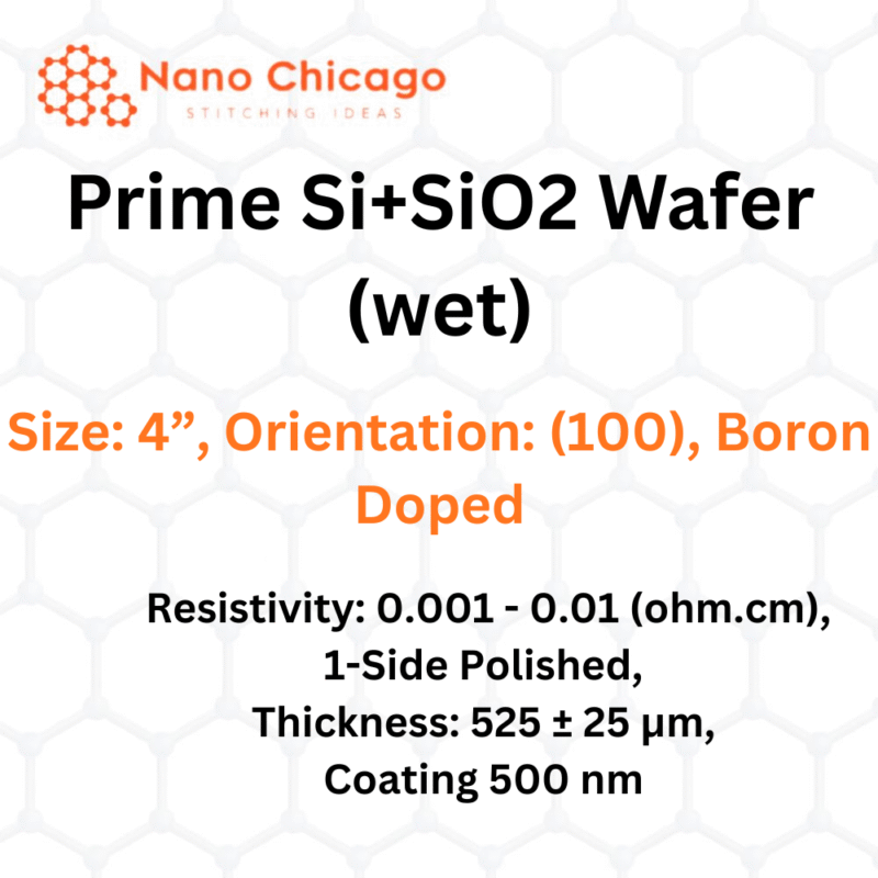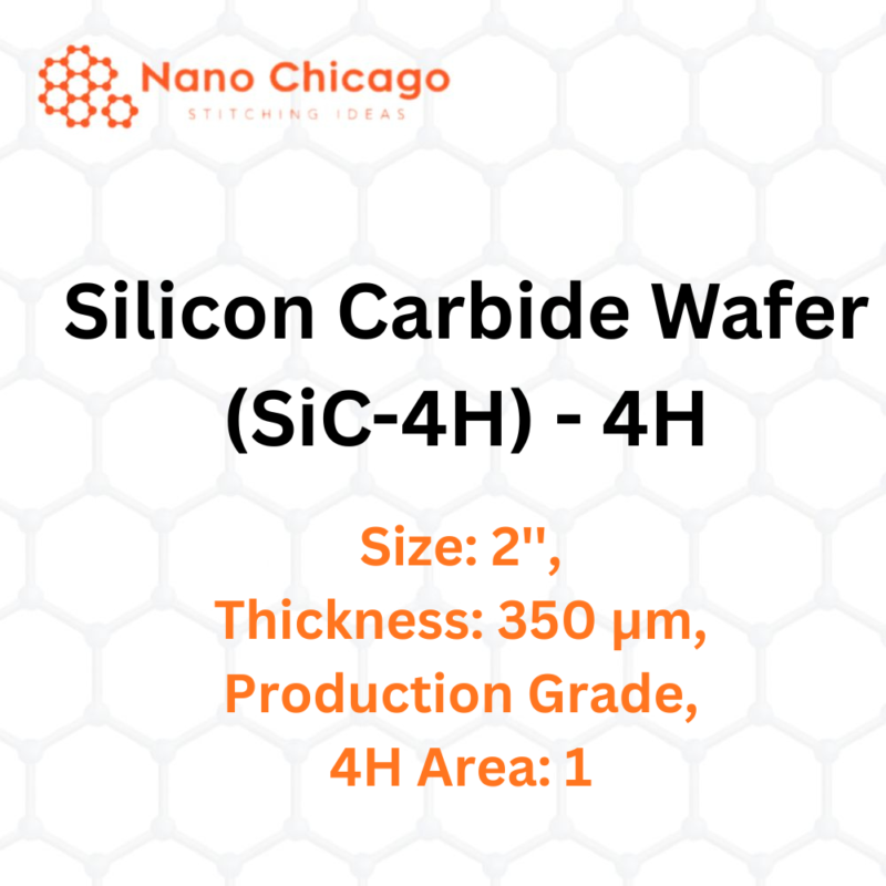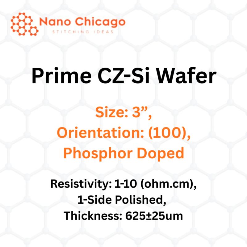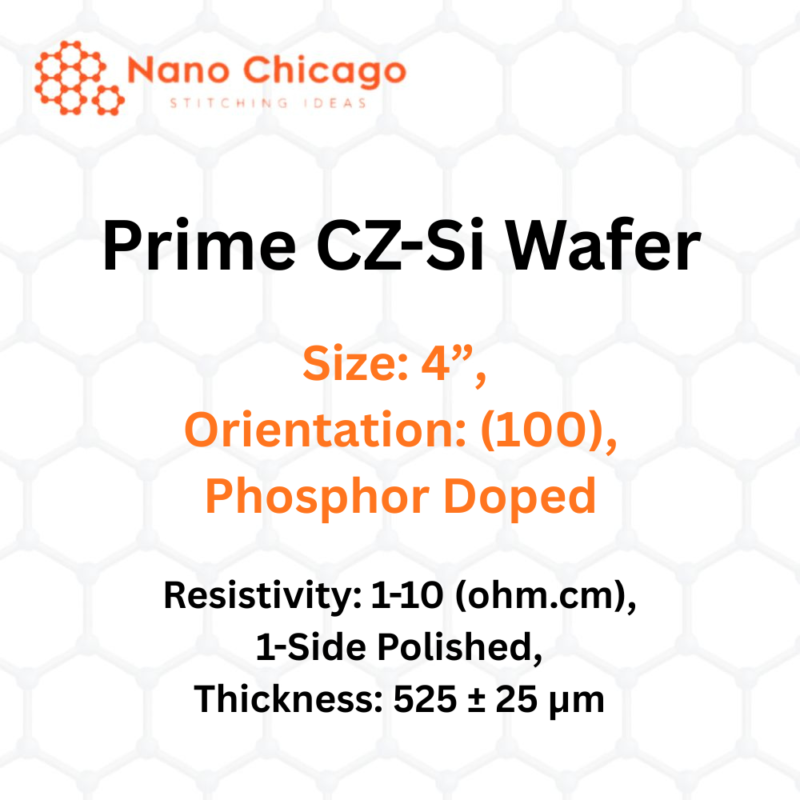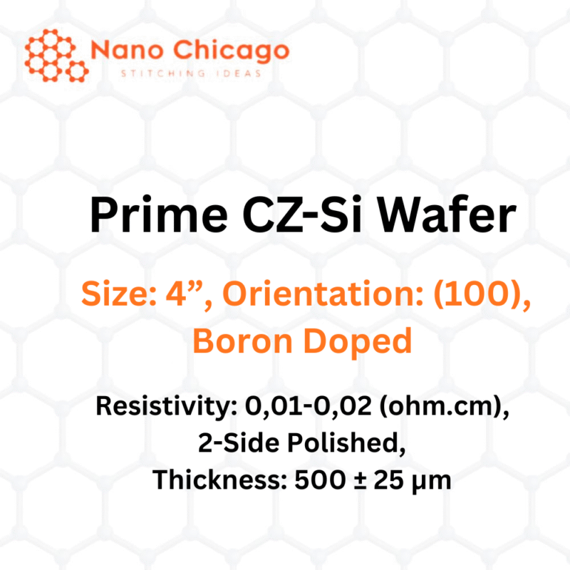
Product Name
Prime CZ-Si Wafer
Specifications
| Property | Specification |
|---|---|
| Quality | Prime |
| Materials | CZ-Si |
| Size (inch) | 4” |
| Orientation | (111) |
| Coating | — |
| Thickness (μm) | 525 ± 25 |
| Doping | Phosphor |
| Resistivity (ohm.cm) | 1-10 |
| Polished | One Side |
Description
Silicon is one of the most common elements in the Earth’s crust. The main usage of silicon wafers is in electronics and technology. Silicon wafers have very flat and mirror-like surfaces. They are produced using the Czochralski method to obtain the highest purity. Depending on the usage area, silicon wafers can be doped with different materials to tailor their purity accordingly. The amount and type of dopants highly affect the electronic properties. Gallium, indium, boron, and nitrogen are some of the dopants used in the production process.
Silicon wafers are widely used in semiconductors, microchips, integrated circuits, smartphones, computers, and other electronic devices. A wafer is a thin slice of semiconductor material that acts as a substrate for microelectronic devices built on and above it.