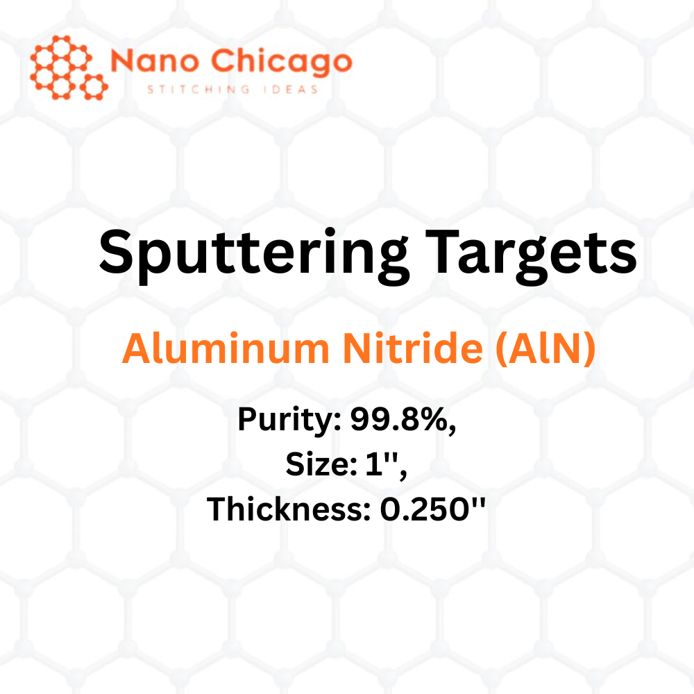
Aluminum Nitride (AlN) Sputtering Targets
Purity: 99.8% Size: 1” Thickness: 0.250”
Aluminum nitride (AlN) sputtering targets enable precise and uniform thin film deposition across diverse substrate shapes and sizes. The sputtering process is repeatable and scalable from R&D to production batches. Chemical reactions can occur on the target surface, in-flight, or on the substrate, depending on process parameters, giving experts control over film growth, microstructure, and material properties.
Applications
-
Thin-Film Deposition:
Deposits AlN films onto substrates like silicon wafers with high uniformity. -
Semiconductor Etching:
Suitable for anisotropic etching where selectivity is not critical. -
Material Analysis (SIMS):
Enables precise measurement of composition and trace impurities. -
Space Applications:
Useful for simulating space weathering processes on airless bodies like asteroids and the Moon. -
Optical & Optoelectronic Devices:
AlN films offer wide band gap (~6.2 eV), high refractive index (~2.0), and low absorption (<10⁻³), ideal for sensors, LEDs, and other optoelectronic applications.
Material Advantages
-
Excellent combination of physical, chemical, and mechanical properties.
-
High thermal and chemical stability suitable for harsh environments.
-
Supports reactive DC magnetron sputtering for reproducible, scalable, and cost-effective film growth.
-
Film properties depend on deposition conditions such as sputtering power, pulse frequency, duty cycle, growth temperature, and gas flow ratio.
AlN sputtering targets are widely used in advanced thin film technologies where precision, stability, and high-quality films are critical.