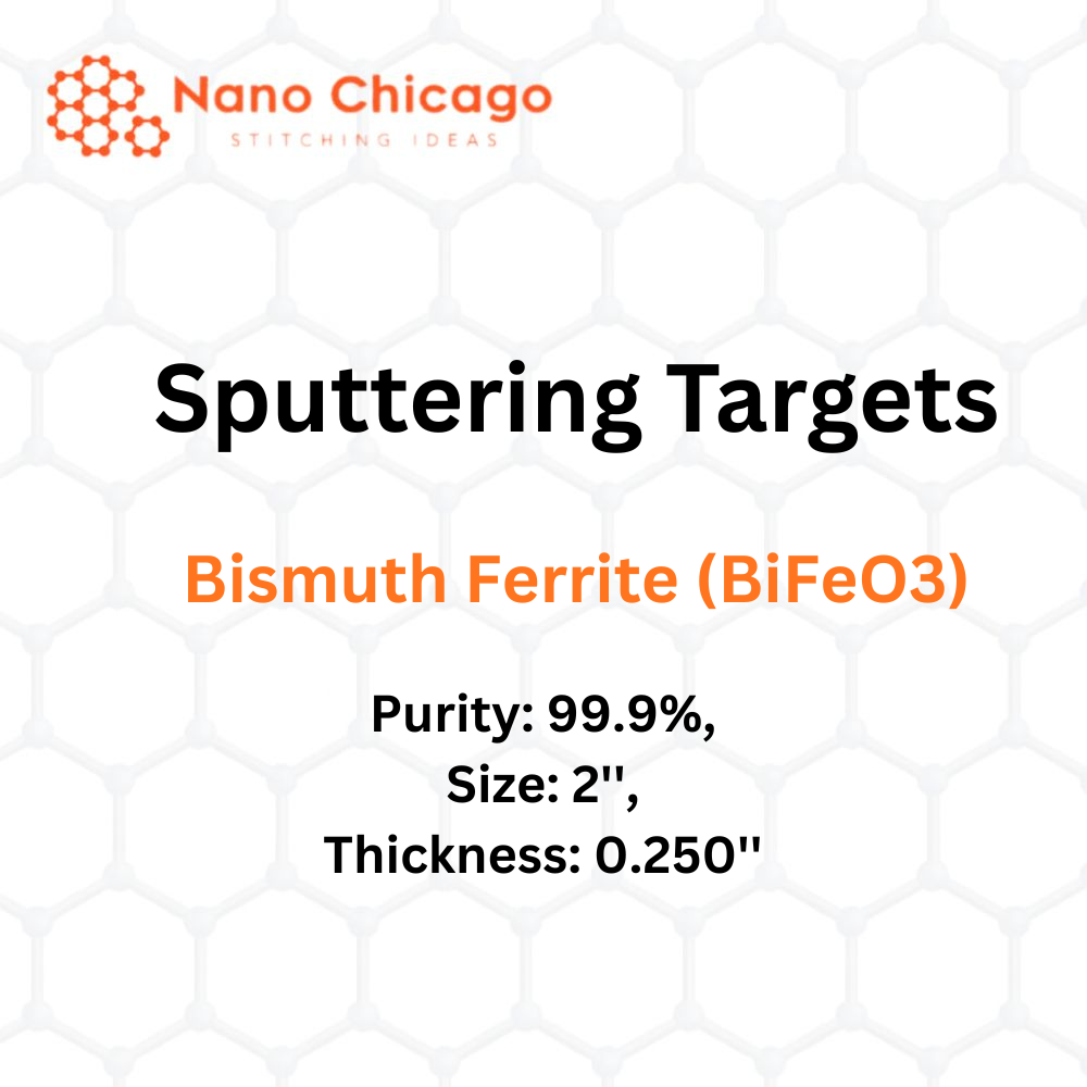
Bismuth Ferrite (BiFeO3) Sputtering Targets, Indium
Purity: 99.9% Size: 2” Thickness: 0.250”
Sputtering is a proven method for depositing thin films from a wide range of materials onto substrates of various shapes and sizes. This process is repeatable and scalable, suitable for small R&D projects as well as medium-to-large production batches. Depending on process parameters, chemical reactions may occur on the target surface, in-flight, or on the substrate, giving experts precise control over film growth and microstructure.
Applications of Sputtering Targets
-
Thin Film Deposition: Deposits material from the target onto substrates such as silicon wafers.
-
Semiconductor Etching: Preferred for cases requiring high etching anisotropy without selectivity concerns.
-
Analytical Uses: Supports techniques like Secondary Ion Mass Spectroscopy (SIMS) for compositional analysis and trace impurity detection.
-
Space Applications: Plays a role in space weathering, altering the physical and chemical properties of airless bodies like asteroids and the Moon.
About Bismuth Ferrite (BiFeO3)
Bismuth ferrite (BiFeO3) is an inorganic perovskite-structured compound and one of the most promising multiferroic materials. Sputtering targets are typically produced via high-temperature sintering or recrystallization of Bi and Fe oxide compounds to achieve single-phase BiFeO3. Indium bonding is recommended for optimal target performance.
This Pb-free ferroelectric material exhibits exceptional properties, including large remnant polarization, high Curie temperature, and high antiferromagnetic Néel temperature. It is unique in combining magnetic and ferroelectric properties at and above room temperature. Its strong polarization-induced photovoltaic response and 3.3 eV direct band gap make BiFeO3 films ideal for advanced ferroelectric photovoltaic research.