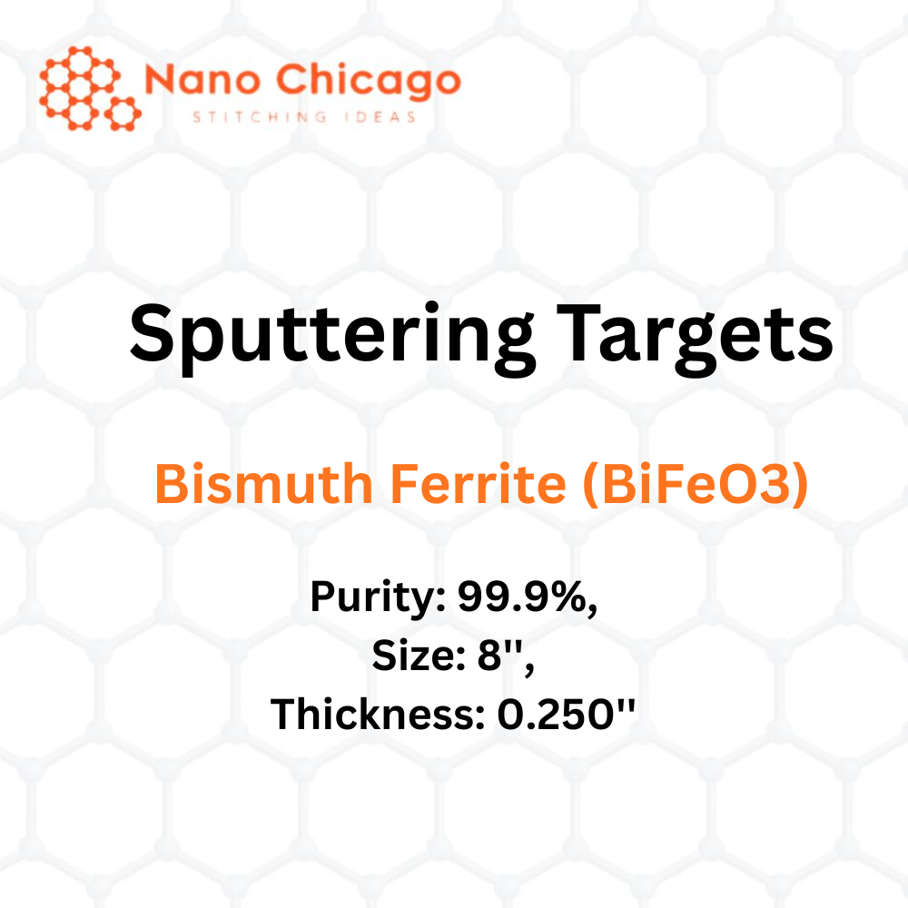
Bismuth Ferrite (BiFeO3) Sputtering Targets, Indium
Purity: 99.9% Size: 8” Thickness: 0.250”
Sputtering is a well-established technique for depositing thin films from a wide variety of materials onto diverse substrate shapes and sizes. The process with sputtering targets is highly repeatable and scalable, supporting both small R&D projects and larger production batches. Chemical reactions can occur on the target surface, in-flight, or on the substrate depending on process parameters. Despite its complexity, sputtering offers precise control over film growth and microstructure.
Applications of Sputtering Targets
-
Thin Film Deposition: Material is eroded from a “target” and deposited onto a “substrate,” such as a silicon wafer.
-
Semiconductor Etching: Sputter etching is used when high anisotropy is required and selectivity is not a concern.
-
Analytical Uses: Gradual target etching enables composition analysis, including detection of very low impurity concentrations, as in Secondary Ion Mass Spectroscopy (SIMS).
-
Space Applications: Sputtering contributes to space weathering, altering physical and chemical properties of airless bodies such as asteroids and the Moon.
About Bismuth Ferrite (BiFeO3)
Bismuth ferrite (BiFeO3) is an inorganic compound with a perovskite structure and is one of the most promising multiferroic materials. Sputtering targets are typically produced by high-temperature sintering or recrystallization of Bi and Fe oxide mixtures to obtain single-phase BiFeO3. Indium bonding is recommended for these targets.
Bismuth ferrite is a Pb-free ferroelectric material noted for its excellent ferroelectric properties, including high remnant polarization, high Curie temperature, and high antiferromagnetic Néel temperature. It is one of the few materials exhibiting both magnetic and ferroelectric behavior at and above room temperature. Its polarization-induced photovoltaic properties, combined with a direct band gap of 3.3 eV, make BiFeO3 films highly suitable for ferroelectric photovoltaic studies, outperforming most other ferroelectric materials.