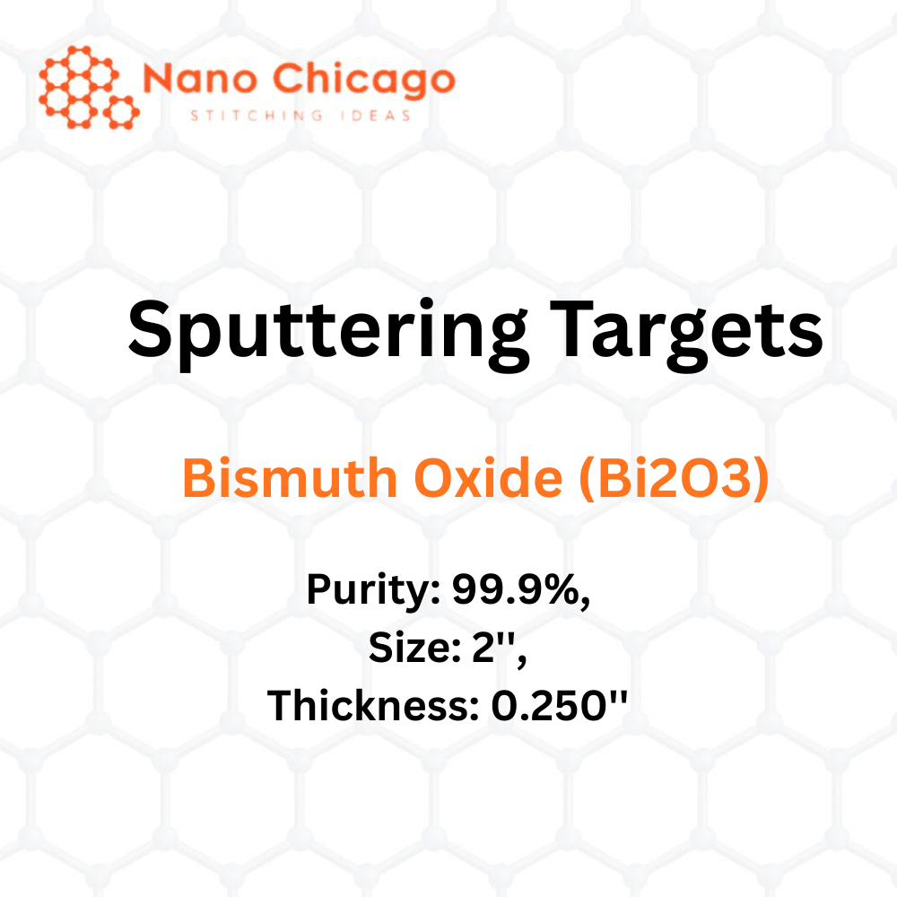
Bismuth Oxide (Bi₂O₃) Sputtering Targets
Purity: 99.9% Size: 2” Thickness: 0.250”
Sputtering is a proven, versatile method for depositing thin films from a wide range of materials onto substrates of various shapes and sizes. The process is highly repeatable and can be scaled from small R&D environments to medium- and large-area production batches. Chemical reactions during sputtering may occur on the target surface, in-flight, or on the substrate depending on process parameters. While this complexity introduces many variables, it also provides experts with exceptional control over film growth and microstructure.
Applications of Sputtering Targets
1. Thin Film Deposition
Sputtering enables the transfer of material from a solid “target” onto a substrate (such as silicon wafers) through controlled erosion. This is widely used for producing uniform, high-quality thin films.
2. Semiconductor Processing
Sputter etching allows precise, anisotropic etching when high directional control is required and selectivity is not the primary concern.
3. Surface and Material Analysis
Techniques such as Secondary Ion Mass Spectrometry (SIMS) use sputtering to remove surface layers at a constant rate. The sputtered atoms are analyzed via mass spectrometry to determine composition and detect very low impurity levels.
4. Space and Planetary Science
Sputtering contributes to space weathering—the process that alters the chemical and physical properties of airless bodies like asteroids and the Moon.
Material Overview: Bismuth Oxide (Bi₂O₃)
Bismuth oxide (Bi₂O₃) is one of the most important bismuth compounds, valued for its notable optical and electrical characteristics:
-
Wide bandgap (2–4 eV)
-
High refractive index
-
High oxygen-ion conductivity at medium and elevated temperatures
These properties make Bi₂O₃ highly suitable for:
-
Optoelectronic devices
-
Solar energy harvesting systems
-
Solid oxide fuel cells (SOFCs)
Bi₂O₃ exists in several polymorphs—α, β, γ, and δ—each with unique structural, optical, and mechanical properties. Only the α-phase (low-temperature monoclinic) and δ-phase (high-temperature cubic) are stable; the others are metastable.
Magnetron Sputtering & Functional Applications
Magnetron sputtering is widely used for Bi₂O₃ due to its high deposition rate, excellent film adhesion, and compatibility with large-area deposition equipment. Bismuth oxide–based films exhibit strong ionic conductivity, making them ideal for:
-
SOFC electrolytes
-
Oxygen sensors
-
Gas sensors
-
Optical coatings
-
Ceramic glass production
Additionally, Bi₂O₃ demonstrates:
-
High dielectric permittivity
-
Photoluminescence
-
Strong visible-light photocatalytic activity (useful for water splitting and decontamination)
Bismuth-containing mixed oxides are also promising in microelectronics due to their high charge carrier mobility and long electron mean free path. Notably, thin Bi films become semiconductors at around 30 nm thickness, further expanding their technological potential.