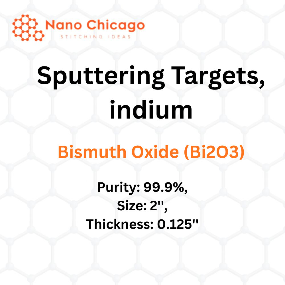
Bismuth Oxide (Bi₂O₃) Sputtering Targets, Indium
Purity: 99.9% Size: 2” Thickness: 0.125”
Sputtering is a reliable and scalable technique for depositing thin films from diverse materials onto substrates of various shapes and sizes. The process allows precise control over film growth and microstructure, with chemical reactions occurring on the target surface, in-flight, or on the substrate depending on parameters. This flexibility makes sputter deposition suitable for both small R&D projects and medium-to-large production batches.
Applications of Sputtering Targets
-
Thin Film Deposition: Transfers material from the target to substrates, such as silicon wafers, forming uniform thin films.
-
Semiconductor Etching: Used for high anisotropy etching where selectivity is less critical.
-
Material Analysis: In secondary ion mass spectrometry (SIMS), sputtering enables measurement of composition and trace impurities.
-
Space Applications: Contributes to space weathering, altering the physical and chemical properties of airless celestial bodies like asteroids and the Moon.
Material Overview
Bismuth oxide (Bi₂O₃) is a key bismuth compound valued for its optical and electrical properties, including a wide energy gap (2–4 eV), high refractive index, and significant oxygen ion conductivity at medium and high temperatures. These properties make it promising for applications in optoelectronics, solar cells, and solid oxide fuel cells (SOFCs).
Bismuth oxide exists in several polymorphic forms (α, β, γ, δ) with distinct crystal structures and properties. Only the α-phase (low-temperature monoclinic) and δ-phase (high-temperature face-centered cubic) are stable, while the others are metastable.
Magnetron sputtering is widely used due to its high deposition rate, dense and adhesive films, and compatibility with large-area systems. Bi₂O₃-based materials are used in:
-
Electrolytes for SOFCs and oxygen sensors
-
Gas sensors and optical coatings
-
Ceramic glass production
-
Photocatalytic applications for water splitting and decontamination
Bismuth-containing oxides also have high electron mobility and long mean free paths, making them suitable for microelectronics. Semi-metal bismuth thin films can even behave as semiconductors at critical thicknesses around 30 nm.