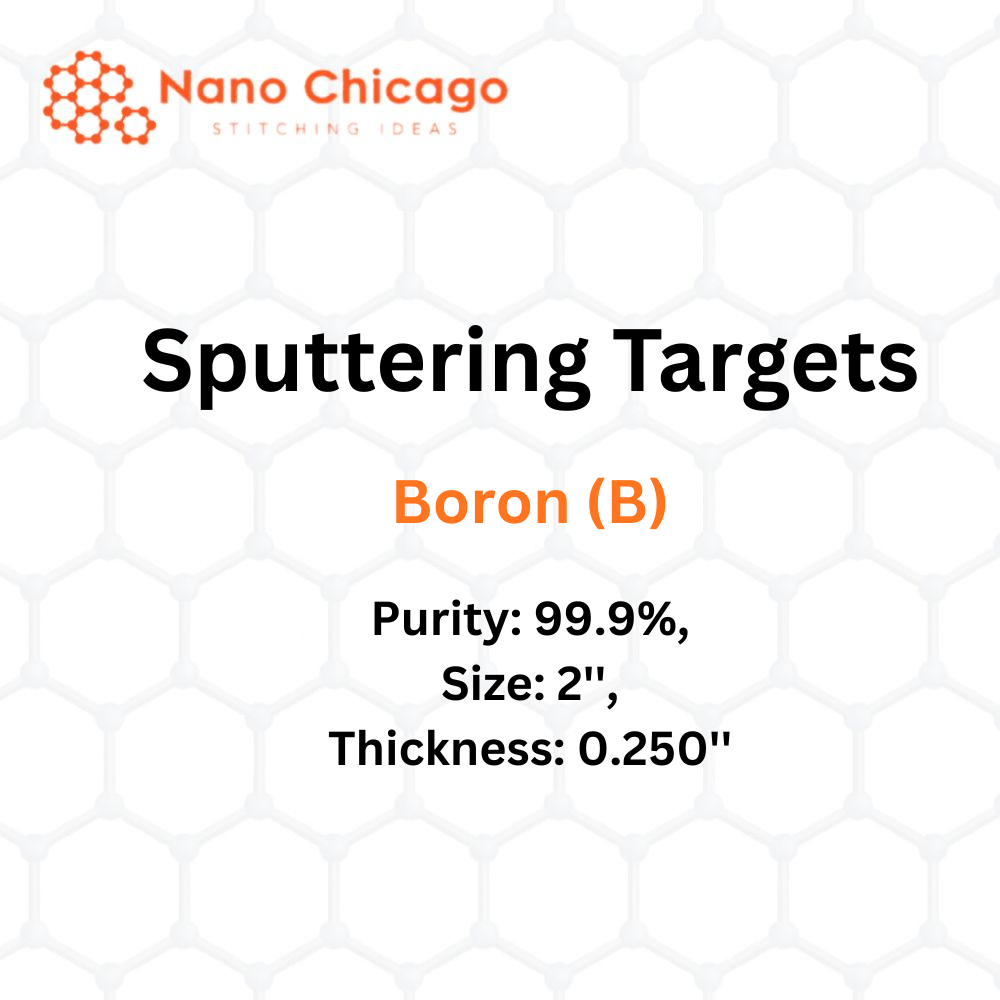
Boron (B) Sputtering Targets
Purity: 99.9%, Size: 2”, Thickness: 0.250”
Product Details
| Parameter | Description |
|---|---|
| Material | Boron (B) |
| Purity | 99.9% |
| Size | 2” |
| Thickness | 0.250” |
| Form | Sputtering Target |
| Manufacturer | Nano Chicago |
| Key Features | Reliable thin film deposition, repeatable and scalable process, precise control over growth and microstructure |
Description
Sputtering is a reliable technique for depositing thin films from a wide range of materials onto various substrate shapes and sizes. The process is repeatable and scalable, suitable for small R&D projects as well as medium-to-large production batches. Depending on process parameters, chemical reactions may occur on the target surface, in-flight, or on the substrate. While sputter deposition involves many variables, it allows precise control over film growth and microstructure.
Boron is widely used for ion-beam doping of semiconductors, surface modification via ion implantation, synthesizing boron-containing films and coatings such as boron nitride, and trench filling in particle detectors. Boron-based coatings enhance surface properties with high hardness, toughness, corrosion and wear resistance, and in some cases, performance comparable to diamond.
Applications
Carbon nanotubes doped with metallic nanopowders provide significant enhancements in both electrical and mechanical performance. These improvements include increased hardness, tensile strength, specific strength, and elastic modulus. As a result, these materials are widely utilized across various fields. Some of these applications include: 1-drug delivery, 2-biosensors, 3-CNT composites, 4-catalysis, 5-nanoprobes, 6-hydrogen storage, 7-lithium batteries, 8-gas-discharge tubes, 9-flat panel displays, 10-supercapacitors, 11-transistors, 12-solar cells, 13-photoluminescence, 14-templates.
-
Thin Film Deposition: Material is eroded from a target and deposited onto substrates such as silicon wafers.
-
Semiconductor Etching: Sputter etching is applied where high anisotropy is required and selectivity is not critical.
-
Analytical Techniques: Secondary ion mass spectrometry (SIMS) uses sputtering to analyze target composition and detect trace impurities.
-
Space Applications: Sputtering contributes to space weathering, modifying the physical and chemical properties of airless bodies like asteroids and the Moon.
-
Boron in Coatings and Thin Films: Ion-beam doping, surface modification, synthesizing boron-containing films, trench filling, and improving hardness, toughness, corrosion and wear resistance.
-
Magnetron Sputtering of Boron: Boron-compound targets produce films with non-boron components aiding film formation or conductivity; pure boron targets are used in semiconductor doping and reactive sputtering of boron nitride films in nitrogen atmosphere.