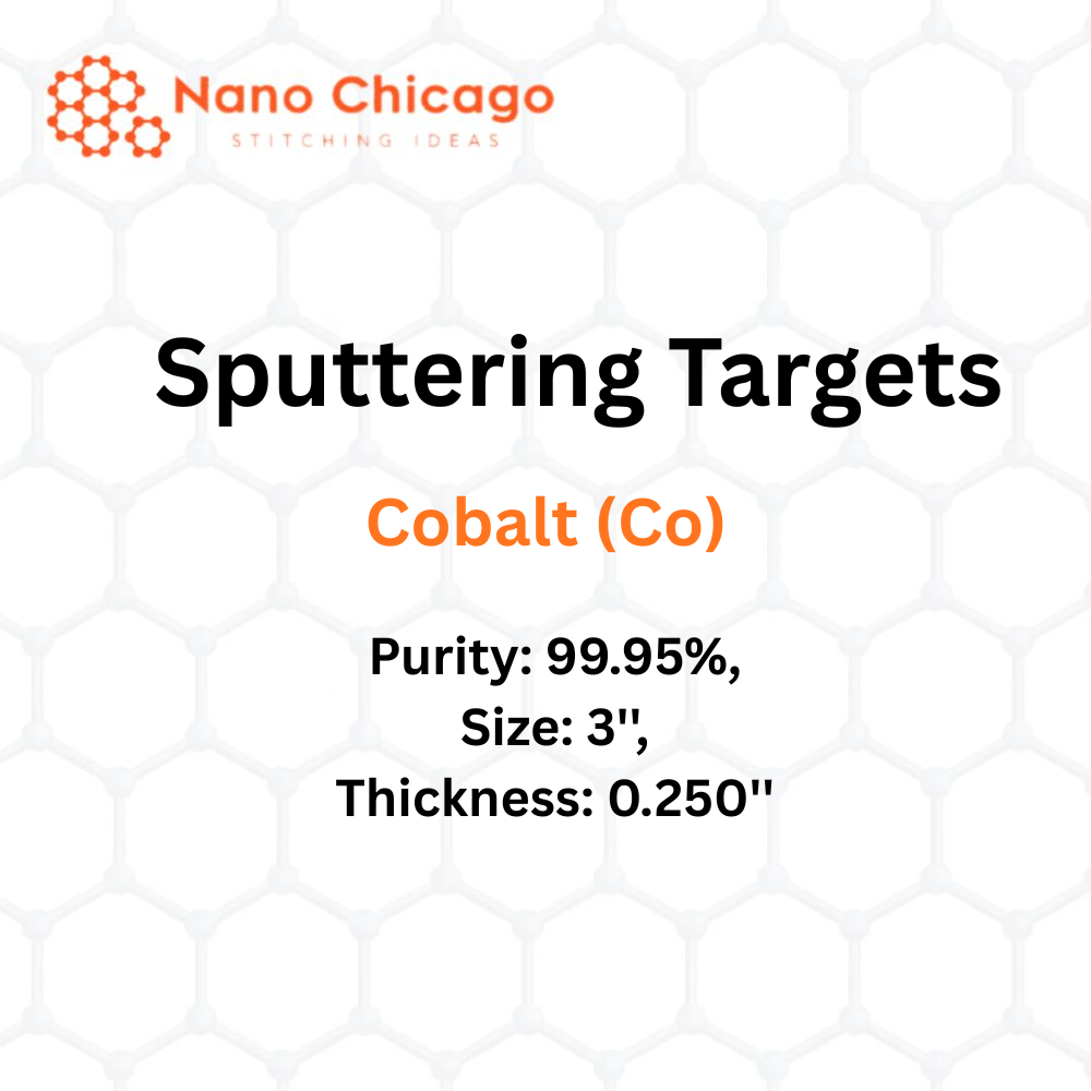
Cobalt (Co) Sputtering Target — Specifications
| Property | Details |
|---|---|
| Material | Cobalt (Co) |
| Purity | 99.95% |
| Size | 3” |
| Thickness | 0.250” |
| Description | Proven sputtering technology for thin-film deposition on diverse substrates. Scalable from R&D to medium/large production. Offers precise control over growth and microstructure. |
Applications of Sputtering Targets
| Application Area | Explanation |
|---|---|
| Film Deposition | Deposits thin films onto substrates like silicon wafers by eroding target material. |
| Semiconductor Etching | Provides high etching anisotropy where selectivity is not critical. |
| Analytical Techniques (SIMS) | Enables composition analysis and detection of trace impurities via mass spectrometry. |
| Space Science | Contributes to space weathering, altering properties of airless bodies like asteroids and the Moon. |
Cobalt-Specific Applications
| Property / Requirement | Explanation |
|---|---|
| Alloy Formation | Forms stable alloys with other metals; suitable for turbine blades and jet engines. |
| Corrosion & Wear Resistance | Suitable for high-strength, wear-resistant applications in industrial and aerospace sectors. |
| Magnetic Properties | One of three room-temperature ferromagnets with uniaxial symmetry; used in magnetic recording and digital data storage. |
| Microelectronics | Thin films for microprocessors, DRAMs, and other semiconductor devices. |
| Dental & Biocompatibility | Used in dental prosthetics to avoid nickel allergies. |
| DC Magnetron Sputtering | Magnetic field traps electrons back to the negatively charged target, enhancing deposition efficiency. |