Product Details
| Property | Specification |
|---|---|
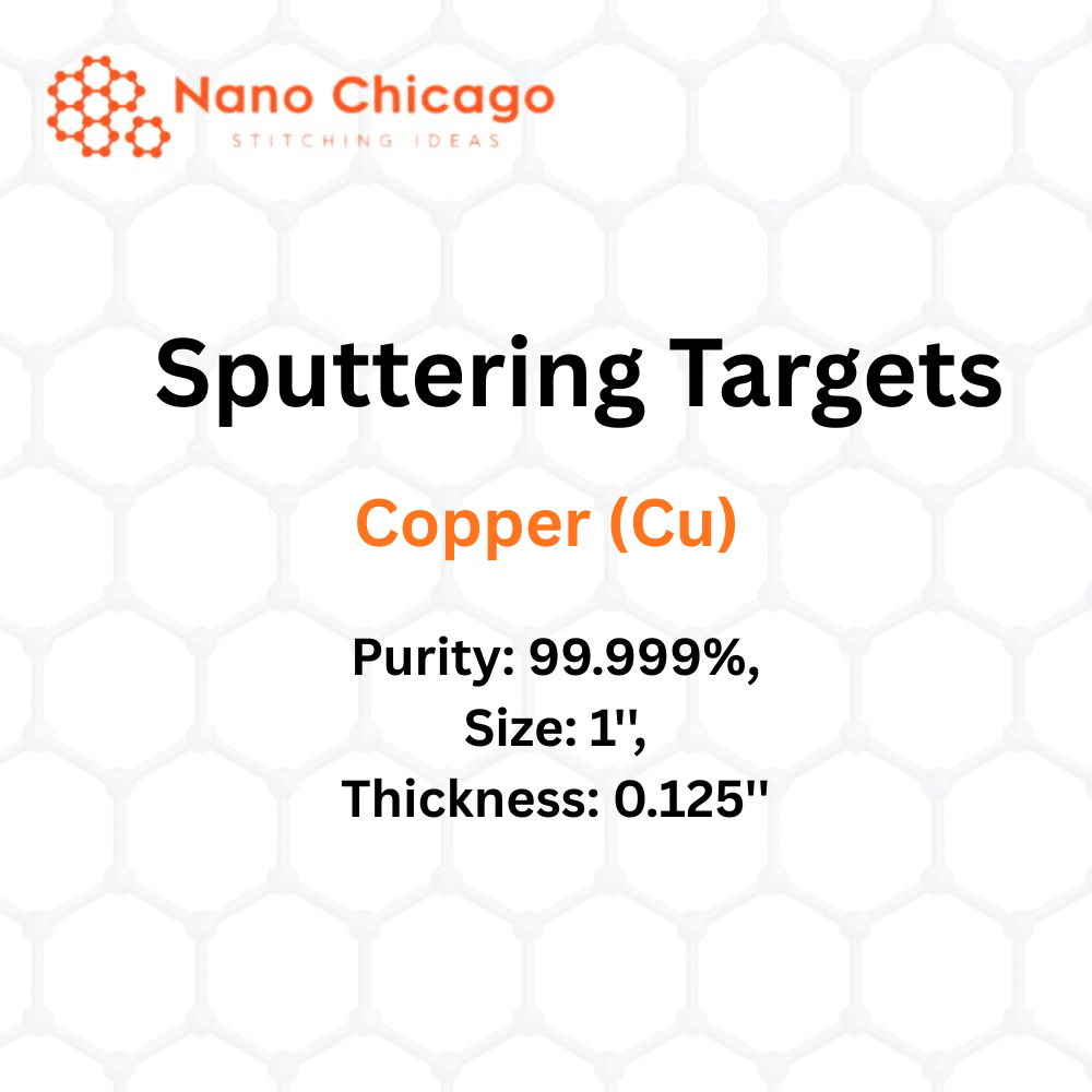
| Product Name | Copper (Cu) Sputtering Target |
| Purity | 99.999% |
| Size | 1” |
| Thickness | 0.125” |
| Description | Sputtering enables deposition of thin films on diverse substrate shapes and sizes. The process is repeatable, scalable from R&D to large production, and allows precise control of film growth and microstructure through adjustable parameters. Chemical reactions may occur on the target, during particle flight, or on the substrate. |
Applications of Sputtering Targets
| Application Area | Description |
|---|---|
| Thin Film Deposition | Material is eroded from the target and deposited onto substrates such as silicon wafers. |
| Semiconductor Processing | Used for sputter etching where high anisotropy is required and selectivity is not critical. |
| Analytical Techniques | Used in SIMS where constant sputtering allows analysis of composition and detection of trace impurities. |
| Space & Planetary Science | Sputtering contributes to space weathering, altering physical and chemical properties of airless bodies like the Moon and asteroids. |